
 My Inquiry
 My Account


Renesas SLG46108V-SKT
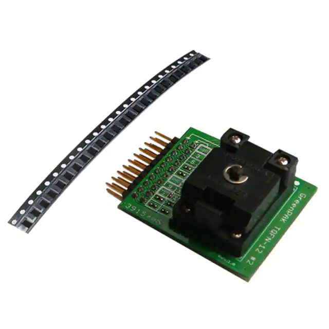
- Part No.:
- SLG46108V-SKT
- Manufacturer:
- Renesas
- Category:
- Programming Adapters, Sockets
- Package:
- Datasheet:
-
 SLG46108V-SKT.pdf
- Description:
- SLG4SA8-10X12 SOCKET ADAPTER
- Quantity:
- Payment:

- Shipping:

Inventory:1,625
Please send an inquiry. Send us your inquiry, and we will respond immediately.
Product details
Overview
SLG46108V-SKT from Renesas Electronics is a one-time programmable (OTP) ultra-small mixed-signal configurable IC implementing logic, timing, filtering, and power management functions in a single STQFN-8 package (1.0 × 1.2 × 0.55 mm). It integrates four LUTs (two 2-bit, two 3-bit), three 8-bit counter/delay generators, RC oscillator (25 kHz or 2 MHz), POR, and six programmable I/O pins - delivering system-level glue logic replacement for space-constrained embedded control applications.
For engineers reviewing the SLG46108V-SKT datasheet, SLG46108V-SKT pinout, SLG46108V-SKT application, or SLG46108V-SKT equivalent, this device serves as a low-power, field-configurable alternative to discrete logic, timers, and level translators in PC peripherals, handheld electronics, and datacom interface conditioning circuits where board area and BOM count reduction are critical.
Technical Context
The SLG46108V-SKT implements a user-programmable interconnect matrix routing signals between six I/O pins and internal macrocells including combinational LUTs, DFF/latch blocks, pipe delay stages, and CNT/DLY units. Its RC oscillator supports auto- and forced-power modes with selectable pre-divider (÷1/÷2/÷4/÷8) and secondary divider (÷1/÷2/÷3/÷4/÷8/÷12/÷24/÷64), enabling precise clock generation without external components.
Each I/O pin supports multiple configurations: digital input (with/without Schmitt trigger or low-voltage mode), push-pull (1X/2X), open-drain NMOS/PMOS (1X/2X), and selectable 10 kΩ/100 kΩ/1 MΩ pull-up or pull-down resistors - with Pin 2 fixed as input-only and Pins 4 & 8 configurable as bidirectional I/O.
Key Specifications
| Parameter | Value and Actual Design Meaning |
|---|---|
| Supply Voltage Range | 1.8 V (±5 %) to 5.0 V (±10 %): Supports direct interfacing with 1.8 V, 3.3 V, and 5 V logic domains without level shifters. |
| Operating Temperature | -40 °C to +85 °C: Qualified for industrial and commercial environments including PC peripherals and portable electronics. |
| I/O Drive Strength | Push-pull 2X: Up to 2.98 mA @ 3.3 V; Open-drain NMOS 2X: Up to 25.46 mA @ 5 V - enables direct LED driving or bus termination. |
| RC Oscillator Accuracy | ±7.66 % over -40 °C to +85 °C at 1.8 V: Sufficient for non-critical timing (e.g., debounce, state machine clocks, wake-up triggers). |
| Typical Propagation Delay | 7.0–10.6 ns (LUT outputs @ 5 V): Enables sub-100 MHz combinational logic operation for real-time signal conditioning. |
| Quiescent Current | 0.28 µA @ 1.8 V (static): Allows battery-powered operation for months in always-on monitoring nodes. |
| Programmability | One-time programmable NVM: Ensures design security and eliminates runtime configuration overhead in production firmware. |
Pinout & Package
Pb-free 8-pin STQFN package: 1.0 mm × 1.2 mm × 0.55 mm body, 0.4 mm pitch, exposed thermal pad (not electrically connected). Compatible with standard reflow profiles and high-density PCB layouts.
| Pin/Terminal | Circuit Role | Design Meaning |
|---|---|---|
| 1 - VDD | Power supply input | Primary power rail; decoupled with 0.1 µF capacitor; split into two sides (Pins 2–4 and 6–8) for noise isolation. |
| 2 - GPI | Dedicated input | General-purpose input only; supports Schmitt-triggered or low-voltage logic; fixed pull-down resistor options. |
| 3 - GPIO | Configurable I/O | Full bidirectional capability: input (Schmitt/no Schmitt/low-V), output (PP/OD-NMOS/OD-PMOS), 1X/2X drive, pull-up/down selection. |
| 4 - GPIO | Configurable I/O | Bidirectional; supports push-pull or open-drain output modes; pull-up/down resistor programmable. |
| 5 - GND | Ground reference | Common return path; split-side grounding matches VDD partitioning to reduce crosstalk between I/O groups. |
| 6 - GPIO | Configurable I/O | Full I/O functionality identical to Pin 3; supports all input/output modes and driver strengths. |
| 7 - GPIO | Configurable I/O | Identical to Pin 3 and Pin 6; enables flexible signal routing across up to five active outputs or inputs. |
| 8 - GPIO | Configurable I/O | Bidirectional; supports same modes as Pin 4; usable as clock input, reset synchronizer, or filtered interrupt source. |
Key Features
| Feature | Design Value |
|---|---|
| Four LUTs (2×2-bit, 2×3-bit) | Enables compact implementation of custom combinational logic (e.g., address decoding, protocol encoding) without external gates. |
| Three independent 8-bit CNT/DLY units | Provides precise, externally clocked delays or counters (1–255 cycles) for timing-critical sequences like power sequencing or pulse stretching. |
| Programmable deglitch filter | Filters input noise down to <35 ns pulses @ 5 V - eliminates false triggers from mechanical switches or noisy sensor lines. |
| RC oscillator with dual-frequency selection | Generates 25 kHz or 2 MHz clocks with on-chip pre- and post-division - replaces external crystal + divider ICs in cost-sensitive designs. |
| Per-pin I/O configuration registers | Allows runtime reconfiguration of input thresholds, drive strength, and pull direction - simplifies prototyping and reduces variant SKUs. |
Applications
| Keyboard/Keypad Debounce | USB Device Power Sequencing |
|---|---|
Use Scenario: Mechanical keypresses generate contact bounce lasting 5–20 ms, causing spurious interrupts in microcontroller-based keyboards. IC Role / Device Role / Timing Role: SLG46108V-SKT acts as a hardware debounce engine using its deglitch filter and programmable delay macrocells to clean inputs before routing to MCU GPIO. Use Value: Eliminates software polling or timer-based debounce routines, reducing MCU firmware complexity and CPU load while ensuring deterministic response. | Use Scenario: USB devices require strict VBUS detection, 100-ms power-rail ramp-up, and controlled enable sequencing for USB PHY, controller, and peripheral ICs. IC Role / Device Role / Timing Role: SLG46108V-SKT implements a state machine using LUTs and CNT/DLY units to monitor VBUS, assert reset signals with calibrated delays, and gate power-enable lines. Use Value: Replaces 3–5 discrete logic ICs and RC networks, shrinking layout area by >70 % and improving timing repeatability across temperature. |
| Industrial Sensor Interface Conditioning | Legacy Display Backlight Control |
Use Scenario: Analog sensors (e.g., thermistors, photoresistors) output noisy, slow-varying signals requiring filtering, threshold comparison, and hysteresis before MCU ADC sampling. IC Role / Device Role / Timing Role: SLG46108V-SKT configures GPIO pins as Schmitt-triggered comparators with programmable hysteresis and filters raw sensor outputs using its deglitch macrocell. Use Value: Provides analog-like behavior in digital domain - no external op-amps or RC filters needed - while maintaining immunity to EMI-induced glitches. | Use Scenario: Older LCD modules require PWM dimming at 100–500 Hz with precise duty-cycle control and soft-start to prevent backlight flicker or inrush current spikes. IC Role / Device Role / Timing Role: SLG46108V-SKT generates stable PWM using its RC oscillator and CNT/DLY units, with programmable start-up ramp via LUT-controlled duty-cycle stepping. Use Value: Delivers flicker-free dimming without MCU intervention or dedicated PWM IC, reducing BOM cost and freeing MCU timers for other tasks. |
Equivalent & Alternatives
The following parts are listed as comparable options for similar programmable mixed-signal logic applications.
| Alternative Part | Technical Difference | Application Difference | Selection Advice |
|---|---|---|---|
| SLG46122V | 10-pin STQFN; adds 2 extra GPIOs and 1 additional CNT/DLY unit; same LUT count and oscillator specs. | Suitable when ≥8 I/Os or dual independent delay chains are required (e.g., dual-sensor synchronization). | Select SLG46122V only if pin count and macrocell expansion justify larger footprint and higher unit cost. |
| SLG46533V | 14-pin TDFN; includes I²C interface, analog comparator, and voltage reference; higher quiescent current (1.2 µA @ 1.8 V). | Required for systems needing analog sensing + digital logic co-processing (e.g., battery voltage monitoring + LED status control). | Choose SLG46533V when I²C configurability or analog front-end integration outweighs size and power penalties. |
Compared with SLG46122V and SLG46533V, the SLG46108V-SKT offers the smallest footprint and lowest static power for pure digital glue logic - making it optimal for ultra-compact, battery-sensitive applications where analog or expanded I/O are unnecessary.
Availability
SLG46108V-SKT is available at Aetrix Electronics and suitable for keyboard debounce, USB power sequencing, industrial sensor interface conditioning, and legacy display backlight control requiring stable component supply and long-term manufacturability.
Supply support for SLG46108V-SKT includes scheduled delivery planning, volume procurement assistance, BOM continuity management, traceable sourcing, and lifecycle availability coordination for OEM customers, industrial embedded developers, connected-device designers, and electronics production programs.
Manufacturer
Renesas Electronics Corporation is a global semiconductor leader delivering microcontrollers, analog, power, and SoC solutions for automotive, industrial, and enterprise applications.
The GreenPAK family - including SLG46108V-SKT - was designed to replace discrete logic, timers, and level translators with field-programmable mixed-signal ICs targeting space-constrained, cost-sensitive embedded control systems.
FAQ
What programming tools are required to configure the SLG46108V-SKT?
The SLG46108V-SKT is programmed using Renesas' free GreenPAK Designer software and a compatible programming adapter (e.g., SLG4DVKLB-817). The tool enables schematic- or text-based design entry, simulation, and OTP programming via the device's I²C-compatible interface. No external programmer license or subscription is required, and on-chip emulation allows functional validation before final NVM programming.
Can the SLG46108V-SKT operate reliably at 1.8 V supply while driving 3.3 V logic inputs?
Yes - the SLG46108V-SKT supports 1.8 V operation and its GPIO pins can be configured as push-pull or open-drain outputs with programmable drive strength. When used as an open-drain NMOS output with external 3.3 V pull-up, it safely interfaces with 3.3 V logic inputs. Its VIH/VIL thresholds scale with VDD, ensuring correct recognition of 3.3 V signals when configured as an input with Schmitt trigger enabled.
Does the SLG46108V-SKT support reprogramming after initial OTP configuration?
No - the SLG46108V-SKT uses one-time programmable (OTP) non-volatile memory. Once programmed, the configuration is permanent and cannot be erased or rewritten. However, GreenPAK Designer supports full on-chip emulation: the design runs dynamically in RAM while powered, allowing unlimited iteration and verification before committing to OTP. This ensures design correctness prior to final programming of SLG46108V-SKT.
How does the RC oscillator accuracy affect timing-critical functions like pulse generation?
The SLG46108V-SKT's RC oscillator exhibits ±7.66 % frequency variation over -40 °C to +85 °C at 1.8 V. For pulse generation, this translates to ±7.7 % timing error in delay or period - acceptable for non-precision tasks like switch debouncing or power sequencing, but insufficient for UART baud rate generation or audio clocking. For such cases, use an external clock input or select a higher-accuracy oscillator variant like SLG46533V with integrated reference.
What is the maximum output current capability of SLG46108V-SKT GPIO pins?
At 5 V supply, SLG46108V-SKT GPIO pins support up to 5.47 mA sink current (open-drain NMOS 2X, VOL = 0.15 V) and 56.32 mA source current (push-pull 2X, VOH = 2.4 V). Total per-side current limits apply: ≤45 mA through VDD and ≤90 mA through GND. These ratings allow direct driving of small LEDs, MOSFET gates, or logic inputs - but not high-current loads like relays or motors without external buffering.
SLG46108V-SKT Specifications
- Product attributes
- Attribute value
- Manufacturer:
- Renesas
- Series:
- GreenPAK™
- Packaging:
- Bag
- Product Status:
- Active
- Module/Board Type:
- Socket Module - QFN
- For Use With/Related Products:
- SLG46108
SLG46108V-SKT FAQ
1.How can I place an order for SLG46108V-SKT through Aetrix?
Please submit a Request for Quotation (RFQ) for SLG46108V-SKT on Aetrix. Our sales agent will provide a competitive quotation and guide you through the order confirmation once you accept the terms.
2.Are the price and stock information for SLG46108V-SKT reliable?
The price and inventory of SLG46108V-SKT are updated periodically and may fluctuate due to market conditions. Stock and pricing data are typically refreshed every 24 hours. Quotation validity for SLG46108V-SKT is usually 5 days.
3.What payment methods are accepted for SLG46108V-SKT?
We accept Wire Transfer, PayPal, Credit Card, Western Union, MoneyGram, and Escrow for SLG46108V-SKT transactions.
Note: Certain payment methods may incur a processing fee.
4.How is shipping managed for SLG46108V-SKT?
SLG46108V-SKT orders can be shipped via leading logistics carriers, including DHL, UPS, FedEx, TNT, or Registered Mail.
Once your SLG46108V-SKT order is processed, you will receive an email with the shipment details and tracking number.
Note: Tracking information may take up to 24 hours to appear. Express delivery typically takes 3–5 business days.
5.How can I obtain technical support or documentation for SLG46108V-SKT?
For technical support, including SLG46108V-SKT datasheets, pinout diagrams, or application guidance, please contact our engineering support team. They can provide detailed documentation and assistance for your SLG46108V-SKT requirements.
6.How does Aetrix verify that SLG46108V-SKT is sourced from the original manufacturer or authorized distributors?
All SLG46108V-SKT products on Aetrix are procured from qualified distributors and authorized channels. Our dedicated quality assurance team conducts strict verification, including traceability checks and, if necessary, third-party testing. This ensures that SLG46108V-SKT meets industry standards.
7.What is the process for return or replacement of SLG46108V-SKT?
All SLG46108V-SKT units undergo pre-shipment inspection (PSI). If there is an issue with SLG46108V-SKT, returns or replacements are accepted under the following conditions:
1.Quantity discrepancies, incorrect items, or visible external defects (such as breakage or corrosion), acknowledged by Aetrix.
2.The issue is reported within 90 days of delivery.
3.The SLG46108V-SKT part is unused and in its original packaging.
Return procedure for SLG46108V-SKT:
1.Submit a request within 90 days.
2.Obtain a Return Material Authorization (RMA) from Aetrix.
SLG46108V-SKT Tags
-
AC102015
Microchip Technology
-
LGA SOCKET SML
Telit Cinterion
-
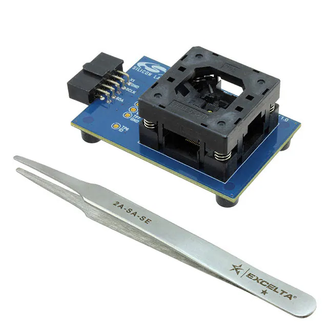
SI5332-32SKT-DK
Skyworks Solutions Inc.
-
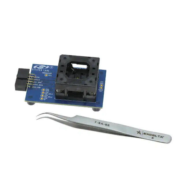
SI5332-40SKT-DK
Skyworks Solutions Inc.
-
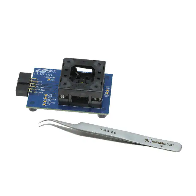
SI538X4X-64SKT-DK
Skyworks Solutions Inc.
-
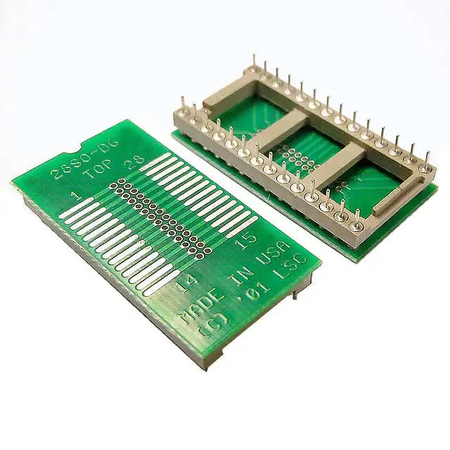
PA-SOD6SM18-28
Logical Systems Inc.
-
SI538X4X-44SKT-DK
Skyworks Solutions Inc.

-
SLG47528V-SKT
Renesas Electronics Operations Services Limited
-
SLG47525V-SKT
Renesas Electronics Operations Services Limited
-
LSOCTS08EA-1
BPM Microsystems
-
ATSTK600-UC3A0X-144
Microchip Technology
-
LSOCS08EA-1
BPM Microsystems
Tech Hub

TTL and CMOS logic families differ in thresholds, loading, output drive, power and timing. This engineering guide compares 74HC and 74HCT, calculates noise margins and checks 3.3 V/5 V compatibility.

A practical engineering guide to 3.3V and 5V logic compatibility, input thresholds, resistor dividers, translator ICs, MOSFET level shifting, I2C pull-ups, timing limits and power-sequencing risks.

The 74HC595 uses push-pull logic outputs, while the TPIC6B595 uses 50 V open-drain DMOS sinks for higher-power loads. This guide compares timing, current limits, 3.3 V interfacing, load wiring, thermal…

The 74HC595 converts serial data into eight stable parallel outputs. This guide covers pin functions, shift and storage timing, OE and MR behavior, drive-current limits, cascading, voltage compatibilit…

A technical comparison of level-sensitive latches and edge-triggered flip-flops, covering timing windows, setup and hold limits, master–slave operation, time borrowing, race-through, HDL inference and…

A D latch stores one bit while Enable controls when data can pass. This reference covers gate-level operation, truth tables, transparency, setup and hold timing, LE versus OE, common ICs and practical …

An SR latch stores one bit through cross-coupled feedback. This engineering reference covers NOR and NAND implementations, truth tables, forbidden-state recovery, gated operation, switch debouncing, fa…

Latch circuits retain one bit through feedback. This technical reference covers SR and D latches, truth tables, transparency, timing limits, latch-versus-flip-flop behavior, applications and common log…

An engineering guide to LED driver operation, constant-current and constant-voltage outputs, linear and switching topologies, dimming, IC selection, calculations, replacement compatibility, and fault c…

Operational amplifier guide covering op amp basics, feedback, ideal vs real op amps, common configurations, buffer circuits, offset, bias current, gain-bandwidth, slew rate, rail-to-rail limits and sel…


