
 My Inquiry
 My Account


Renesas SLG46620V-SKT
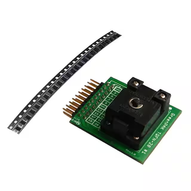
- Part No.:
- SLG46620V-SKT
- Manufacturer:
- Renesas
- Category:
- Programming Adapters, Sockets
- Package:
- Datasheet:
-
 SLG46620V-SKT.pdf
- Description:
- SLG4SA20-20X30 SOCKET ADAPTER
- Quantity:
- Payment:

- Shipping:

Inventory:4,858
Please send an inquiry. Send us your inquiry, and we will respond immediately.
Product details
Overview
SLG46620V-SKT from Renesas Electronics is a one-time-programmable (OTP) GreenPAK mixed-signal matrix IC featuring 25 LUTs (8×2-bit, 16×3-bit, 1×4-bit), six analog comparators, an 8-bit SAR ADC with 3-bit PGA, two DACs, and dual internal voltage references. It operates from 1.8 V to 5.0 V across –40°C to +85°C and supports programmable delays, counters, DFFs, and three internal oscillators (LF, RC 25 kHz/2 MHz, ring). It serves as a configurable logic-and-analog subsystem in power management sequencing and sensor interface circuits.
For engineers reviewing the SLG46620V-SKT datasheet, SLG46620V-SKT pinout, SLG46620V-SKT application, or SLG46620V-SKT equivalent, this device enables rapid prototyping of custom mixed-signal functions without ASIC development-ideal for low-power embedded control, I/O expansion, and analog threshold detection where flexibility, small footprint (2×3 mm STQFN-20), and OTP configuration security are critical.
Technical Context
The SLG46620V-SKT implements a fully user-configurable interconnect matrix routing signals between 20 GPIO pins and 25 combinatorial LUTs, ten CNT/DLY macrocells (including wake-sleep control and FSM variants), twelve DFF/latches, two pipe delays, and six ACMPs with shared input multiplexing. Its architecture supports both digital logic synthesis and analog signal conditioning within a single die.
It integrates three independent oscillators (low-frequency, RC at 25 kHz or 2 MHz, ring), bandgap references, POR, and slave SPI for configuration readback and emulation. The NVM is OTP but supports on-chip emulation via GreenPAK Designer-allowing iterative design validation before final programming.
Key Specifications
| Parameter | Value and Actual Design Meaning |
|---|---|
| Supply Voltage Range | 1.8 V (±5%) to 5.0 V (±10%) - supports direct interfacing with 1.8 V, 3.3 V, and 5 V logic domains without level shifters. |
| Operating Temperature | –40°C to +85°C - qualified for industrial and consumer equipment environments including PC peripherals and handheld electronics. |
| ADC Resolution | 8-bit SAR with 3-bit PGA - enables precise analog sensing (e.g., battery voltage, thermistor) with programmable gain up to 4×. |
| Comparator Count | Six ACMPs with shared inputs and selectable hysteresis - allows multi-threshold monitoring (e.g., overvoltage, undervoltage, window detection) using minimal pins. |
| LUT Resources | 25 LUTs (8×2-bit, 16×3-bit, 1×4-bit) - sufficient for implementing state machines, glue logic, PWM generators, and combinational control functions. |
| Delay Macrocells | Two programmable delays (PDLY0/PDLY1) with edge detection and up to 4-stage cascading - supports precise timing alignment, pulse stretching, and wake-up delay generation. |
| Package | 20-pin STQFN (2 × 3 × 0.55 mm, 0.4 mm pitch) - ultra-compact surface-mount package optimized for space-constrained PCB layouts. |
Pinout & Package
SLG46620V-SKT is housed in a 20-pin STQFN package measuring 2 mm × 3 mm × 0.55 mm with 0.4 mm pitch. Pin numbering follows standard top-view orientation with Pin 1 at top-left corner.
| Pin/Terminal | Circuit Role | Design Meaning |
|---|---|---|
| 1 | VDD | Main power supply input; powers both analog and digital sections (1.8–5.0 V). |
| 2 | GPI | General-purpose input only; also serves as external reset and ADC clock source. |
| 3–7, 8–10, 12–20 | GPIO | Configurable bidirectional I/O with optional output enable; multiple pins support ACMP+/−, PGA inputs, VREF outputs, and AIN MUX routing. |
| 11 | GND | Digital ground reference; forms one side of split power rail (Pins 2–10 share VDD/GND side A). |
Key Features
| Feature | Design Value |
|---|---|
| OTP NVM Configuration | Enables permanent, tamper-resistant logic/analog configuration after final design validation-no external memory required. |
| Programmable Gain Amplifier | 3-bit PGA integrated with ADC path allows dynamic range optimization for varying sensor output amplitudes without external op-amps. |
| Slave SPI Interface | Supports non-invasive read-back of configuration and real-time emulation debugging-eliminates need for dedicated programming hardware during development. |
| Dual Internal Voltage References | VrefO_0 and VrefO_1 provide stable 1.2 V references for ADC, ACMPs, and DACs-reducing BOM count and layout complexity. |
| Multi-Oscillator System | Three independent clocks (LF, RC 25 kHz/2 MHz, ring) allow trade-offs between accuracy, power, and speed-enabling ultra-low-power sleep modes and high-speed sampling. |
Applications
| Power Sequencing Controller | Sensor Signal Conditioner |
|---|---|
|
Use Scenario: Managing startup/shutdown order of multiple voltage rails in PCs, servers, or FPGA-based systems. IC Role / Device Role / Timing Role: Configurable logic engine that monitors reset lines, generates timed enable pulses, and asserts fault flags based on comparator thresholds. Use Value: Replaces discrete timers, comparators, and logic gates-reducing component count by >70% while enabling field-upgradable sequencing behavior. |
Use Scenario: Converting analog sensor outputs (e.g., temperature, light, pressure) into digital events or PWM-modulated drive signals. IC Role / Device Role / Timing Role: Mixed-signal hub performing PGA amplification, ADC digitization, threshold comparison, and pulse-width modulation-all within one chip. Use Value: Eliminates need for external op-amps, reference ICs, and microcontroller firmware-cutting latency and power vs. software-based solutions. |
| USB-C Port Manager | Industrial I/O Expander |
|
Use Scenario: Detecting cable insertion, negotiating power delivery contracts, and managing VBUS discharge paths in portable devices. IC Role / Device Role / Timing Role: Real-time comparator-based monitoring of CC line voltages, combined with programmable delays for USB PD timing compliance. Use Value: Meets USB PD specification timing windows (e.g., tCCDebounce, tSafe0V) using on-die delays-no external RC networks needed. |
Use Scenario: Adding isolated, configurable digital I/O and analog monitoring capability to PLC modules or motor drives. IC Role / Device Role / Timing Role: Programmable logic block handling input debouncing, LED driver timing, fault latching, and analog watchdog functions. Use Value: Provides deterministic response (<15 ns LUT delay at 5 V) and immunity to EMI-induced glitches via Schmitt-trigger inputs. |
Equivalent & Alternatives
The following parts are listed as comparable options for similar programmable mixed-signal applications.
| Alternative Part | Technical Difference | Application Difference | Selection Advice |
|---|---|---|---|
| SLG46621V | Same GreenPAK family; adds 12-bit SAR ADC and higher-resolution DACs but removes one ACMP and reduces LUT count to 20. | Better suited for precision measurement applications requiring >8-bit resolution; less optimal for multi-comparator thresholding. | Select SLG46621V only if higher ADC/DAC resolution outweighs loss of comparator count and logic density. |
| SLG46533V | Smaller variant: 14-pin STQFN, 12 LUTs, 4 ACMPs, no ADC or DAC; lower quiescent current (0.19 µA typical at 1.8 V). | Ideal for pure digital glue logic or low-power wake-up controllers where analog functions are unnecessary. | Choose SLG46533V when system requires only basic logic, timing, and voltage monitoring-avoiding cost and complexity of unused analog blocks. |
Compared with SLG46620V-SKT, SLG46621V trades analog precision for reduced logic capacity, while SLG46533V sacrifices all data converters and half the comparators to achieve lower power and smaller size-making SLG46620V-SKT the balanced choice for mixed-signal applications demanding both logic density and analog integration.
Availability
SLG46620V-SKT is available at Aetrix Electronics and suitable for personal computers and servers, PC peripherals, and handheld electronics requiring stable component supply, long-term lifecycle support, and RoHS-compliant packaging.
Supply support for SLG46620V-SKT includes scheduled delivery planning, volume procurement assistance, BOM continuity management, traceable sourcing, and lifecycle availability coordination for OEM customers, industrial embedded developers, connected-device designers, and electronics production programs.
Manufacturer
Renesas Electronics Corporation is a global semiconductor leader delivering microcontrollers, analog power, and SoC solutions for automotive, industrial, and enterprise markets.
The GreenPAK product line delivers field-programmable mixed-signal ICs targeting rapid customization of analog and digital functions in space- and power-constrained embedded systems.
FAQ
What is the primary function of the SLG46620V-SKT?
The SLG46620V-SKT is a programmable mixed-signal matrix IC that combines digital logic (25 LUTs, counters, DFFs), analog functions (six ACMPs, 8-bit SAR ADC with 3-bit PGA, two DACs), and timing resources (three oscillators, programmable delays) into a single OTP-configurable device. It replaces discrete logic, comparators, and interface circuitry in compact embedded systems.
Does the SLG46620V-SKT support in-system reprogramming?
No-the SLG46620V-SKT uses one-time-programmable (OTP) NVM. However, Renesas GreenPAK Designer enables full on-chip emulation: users can configure, test, and debug logic and analog behavior dynamically while powered, without committing to OTP until design validation is complete. Once programmed, the SLG46620V-SKT retains its configuration permanently.
Can the SLG46620V-SKT operate from a 2.5 V supply?
Yes-the SLG46620V-SKT supports supply voltages from 1.8 V (±5%) to 5.0 V (±10%), which includes 2.5 V within specification. Electrical characteristics such as VIH/VIL thresholds, output drive strength, and ACMP input ranges are guaranteed across this full range, enabling interoperability with 2.5 V logic families without level translation.
How many analog comparators does the SLG46620V-SKT include, and how are their inputs routed?
The SLG46620V-SKT includes six analog comparators (ACMP0–ACMP5). Inputs are flexibly routed via shared GPIO pins: for example, Pin 6 accepts ACMP0(+) through ACMP4(+), Pin 7 supports ACMP0(–) through ACMP1(–) and PGA_OUT, and Pins 8–10, 12–15 provide additional differential and single-ended ACMP input paths-all configurable in GreenPAK Designer.
Is the SLG46620V-SKT pin-compatible with other GreenPAK devices?
No-SLG46620V-SKT has a unique 20-pin STQFN footprint and pin assignment optimized for its macrocell set and I/O routing. While other GreenPAK devices like SLG46621V share the same package outline, their pin functions differ significantly due to variations in internal resource allocation (e.g., ADC presence, comparator count, LUT topology), making direct PCB replacement impossible without redesign.
SLG46620V-SKT Specifications
- Product attributes
- Attribute value
- Manufacturer:
- Renesas
- Series:
- GreenPAK™
- Packaging:
- Bag
- Product Status:
- Active
- Module/Board Type:
- Socket Module - QFN
- For Use With/Related Products:
- SLG46620
SLG46620V-SKT FAQ
1.How can I place an order for SLG46620V-SKT through Aetrix?
Please submit a Request for Quotation (RFQ) for SLG46620V-SKT on Aetrix. Our sales agent will provide a competitive quotation and guide you through the order confirmation once you accept the terms.
2.Are the price and stock information for SLG46620V-SKT reliable?
The price and inventory of SLG46620V-SKT are updated periodically and may fluctuate due to market conditions. Stock and pricing data are typically refreshed every 24 hours. Quotation validity for SLG46620V-SKT is usually 5 days.
3.What payment methods are accepted for SLG46620V-SKT?
We accept Wire Transfer, PayPal, Credit Card, Western Union, MoneyGram, and Escrow for SLG46620V-SKT transactions.
Note: Certain payment methods may incur a processing fee.
4.How is shipping managed for SLG46620V-SKT?
SLG46620V-SKT orders can be shipped via leading logistics carriers, including DHL, UPS, FedEx, TNT, or Registered Mail.
Once your SLG46620V-SKT order is processed, you will receive an email with the shipment details and tracking number.
Note: Tracking information may take up to 24 hours to appear. Express delivery typically takes 3–5 business days.
5.How can I obtain technical support or documentation for SLG46620V-SKT?
For technical support, including SLG46620V-SKT datasheets, pinout diagrams, or application guidance, please contact our engineering support team. They can provide detailed documentation and assistance for your SLG46620V-SKT requirements.
6.How does Aetrix verify that SLG46620V-SKT is sourced from the original manufacturer or authorized distributors?
All SLG46620V-SKT products on Aetrix are procured from qualified distributors and authorized channels. Our dedicated quality assurance team conducts strict verification, including traceability checks and, if necessary, third-party testing. This ensures that SLG46620V-SKT meets industry standards.
7.What is the process for return or replacement of SLG46620V-SKT?
All SLG46620V-SKT units undergo pre-shipment inspection (PSI). If there is an issue with SLG46620V-SKT, returns or replacements are accepted under the following conditions:
1.Quantity discrepancies, incorrect items, or visible external defects (such as breakage or corrosion), acknowledged by Aetrix.
2.The issue is reported within 90 days of delivery.
3.The SLG46620V-SKT part is unused and in its original packaging.
Return procedure for SLG46620V-SKT:
1.Submit a request within 90 days.
2.Obtain a Return Material Authorization (RMA) from Aetrix.
SLG46620V-SKT Tags
-
AC102015
Microchip Technology
-
LGA SOCKET SML
Telit Cinterion
-
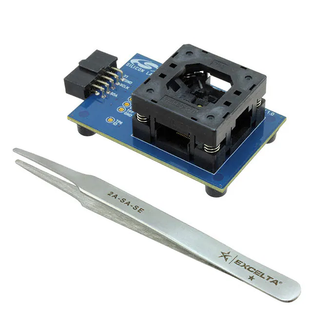
SI5332-32SKT-DK
Skyworks Solutions Inc.
-
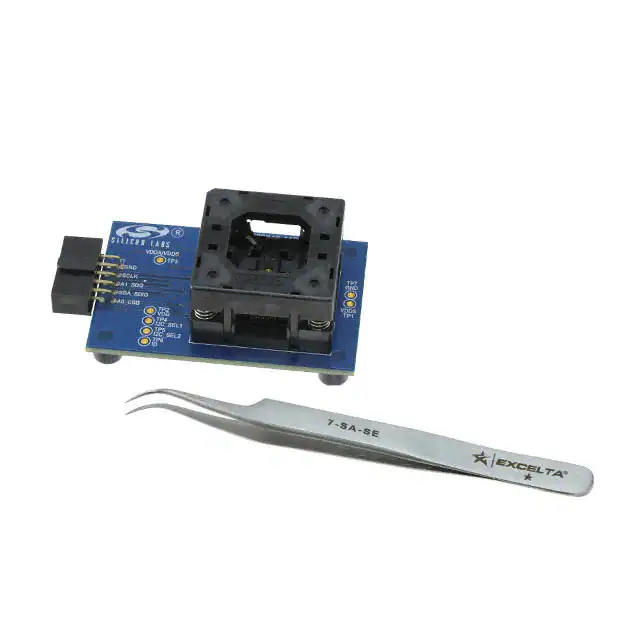
SI5332-40SKT-DK
Skyworks Solutions Inc.
-
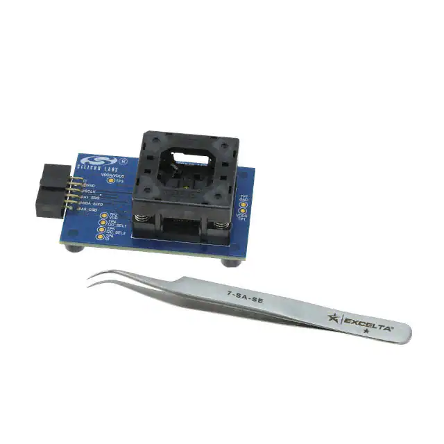
SI538X4X-64SKT-DK
Skyworks Solutions Inc.
-
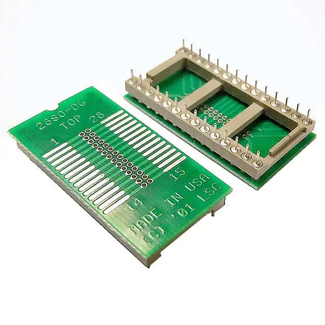
PA-SOD6SM18-28
Logical Systems Inc.
-
SI538X4X-44SKT-DK
Skyworks Solutions Inc.

-
SLG47528V-SKT
Renesas Electronics Operations Services Limited
-
SLG47525V-SKT
Renesas Electronics Operations Services Limited
-
LSOCTS08EA-1
BPM Microsystems
-
ATSTK600-UC3A0X-144
Microchip Technology
-
LSOCS08EA-1
BPM Microsystems
Tech Hub

TTL and CMOS logic families differ in thresholds, loading, output drive, power and timing. This engineering guide compares 74HC and 74HCT, calculates noise margins and checks 3.3 V/5 V compatibility.

A practical engineering guide to 3.3V and 5V logic compatibility, input thresholds, resistor dividers, translator ICs, MOSFET level shifting, I2C pull-ups, timing limits and power-sequencing risks.

The 74HC595 uses push-pull logic outputs, while the TPIC6B595 uses 50 V open-drain DMOS sinks for higher-power loads. This guide compares timing, current limits, 3.3 V interfacing, load wiring, thermal…

The 74HC595 converts serial data into eight stable parallel outputs. This guide covers pin functions, shift and storage timing, OE and MR behavior, drive-current limits, cascading, voltage compatibilit…

A technical comparison of level-sensitive latches and edge-triggered flip-flops, covering timing windows, setup and hold limits, master–slave operation, time borrowing, race-through, HDL inference and…

A D latch stores one bit while Enable controls when data can pass. This reference covers gate-level operation, truth tables, transparency, setup and hold timing, LE versus OE, common ICs and practical …

An SR latch stores one bit through cross-coupled feedback. This engineering reference covers NOR and NAND implementations, truth tables, forbidden-state recovery, gated operation, switch debouncing, fa…

Latch circuits retain one bit through feedback. This technical reference covers SR and D latches, truth tables, transparency, timing limits, latch-versus-flip-flop behavior, applications and common log…

An engineering guide to LED driver operation, constant-current and constant-voltage outputs, linear and switching topologies, dimming, IC selection, calculations, replacement compatibility, and fault c…

Operational amplifier guide covering op amp basics, feedback, ideal vs real op amps, common configurations, buffer circuits, offset, bias current, gain-bandwidth, slew rate, rail-to-rail limits and sel…


