
 My Inquiry
 My Account


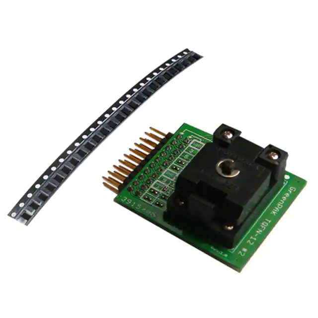
Renesas SLG46722V-SKT
- Part No.:
- SLG46722V-SKT
- Manufacturer:
- Renesas
- Category:
- Programming Adapters, Sockets
- Package:
- Datasheet:
-
 SLG46722V-SKT.pdf
- Description:
- SLG4SA20-20X30 SOCKET ADAPTER
- Quantity:
- Payment:

- Shipping:

Inventory:4,099
Please send an inquiry. Send us your inquiry, and we will respond immediately.
Product details
Overview
SLG46722V-SKT from Silego Technology (now Renesas) is a one-time-programmable mixed-signal array with 15 LUTs (5×2-bit, 9×3-bit, 1×4-bit), eight counter/delay generators, six D flip-flops, and an integrated RC oscillator supporting 25 kHz or 2 MHz operation. It operates from 1.8 V to 5 V and delivers programmable logic, deglitch filtering, and configurable I/O for embedded glue logic replacement in PC peripherals and portable electronics.
For engineers reviewing the SLG46722V-SKT datasheet, SLG46722V-SKT pinout, SLG46722V-SKT application, or SLG46722V-SKT equivalent, this device supports user-defined combinational/sequential logic synthesis via GreenPAK Designer software, offers 18 GPIOs with Schmitt-trigger inputs and 4X super-drive NMOS outputs, and enables rapid prototyping of timing-critical signal conditioning functions without FPGA complexity.
Technical Context
The SLG46722V-SKT implements a fully configurable digital fabric using a connection matrix that routes signals between macrocells-including LUTs, counters, DFFs, and deglitch filters-based on OTP configuration. Its RC oscillator provides two selectable frequencies with programmable pre-dividers, and its 18 GPIOs support multiple input modes (Schmitt-triggered, low-voltage) and output modes (push-pull, open-drain NMOS/PMOS, 1X/2X/4X drive).
Logic functionality is realized through 15 LUTs (five 2-bit, nine 3-bit, one 4-bit), two combination-function macrocells (each offering FF/latch or LUT selection), and eight independent CNT/DLY blocks-including two 14-bit and six 8-bit units-with external clock/reset capability. All macrocells are interconnected via a user-defined routing matrix and configured via non-volatile memory.
Key Specifications
| Parameter | Value and Actual Design Meaning |
|---|---|
| Supply Voltage Range | 1.8 V (±5%) to 5 V (±10%): Enables direct interface with 1.8 V, 3.3 V, and 5 V logic domains without level shifters. |
| Operating Temperature | -40°C to +85°C: Qualified for industrial and commercial environments including PC peripherals and handheld devices. |
| RC Oscillator Frequencies | 25 kHz or 2 MHz: Provides internal clock source for timing functions without external crystal; supports pre-divider chains for sub-harmonic generation. |
| GPIO Count & Flexibility | 18 multi-function pins: 17 support bidirectional I/O with programmable pull-up/down resistors (10 kΩ/100 kΩ/1 MΩ); Pin 2 is input-only. |
| Output Drive Strength | Up to 40 mA NMOS super-drive: Allows direct driving of LEDs, small relays, or capacitive loads without external buffers. |
| Delay Resolution | Programmable delay with 125 ns / 250 ns / 375 ns / 500 ns steps at 3.3 V: Enables precise edge detection and pulse shaping for debouncing or timing alignment. |
| Filter Macrocells | Two deglitch filters: Each provides configurable minimum pulse width rejection (e.g., <35 ns at 5 V) to suppress contact bounce or noise on critical control lines. |
Pinout & Package
SLG46722V-SKT is housed in a 20-pin STQFN package measuring 2 mm × 3 mm × 0.55 mm with 0.4 mm pitch. The package supports high-density PCB layouts and reflow soldering per JEDEC J-STD-020.
| Pin/Terminal | Circuit Role | Design Meaning |
|---|---|---|
| Pin 1 (VDD) | Power supply input | Primary power rail for core and I/O; accepts 1.8–5 V with ±5% to ±10% tolerance depending on nominal voltage. |
| Pin 2 (GPI) | Digital input only | Fixed-input pin with configurable Schmitt trigger or low-voltage mode; used for reset, enable, or sensor interface signals. |
| Pins 3–20 (GPIO) | Multi-function I/O | 17 pins support input/output modes, programmable pull resistors, and output types (push-pull, open-drain NMOS/PMOS, 1X/2X/4X drive). |
| Pin 11 (GND) | Ground reference | Common return path for all internal circuitry and I/O; must be connected to system ground plane for stable operation. |
| Pins 16–20 (Prog) | Programming interface | In programming mode, these pins serve as SCL, SRDWB, SDIO, ID, and mode control for OTP configuration via GreenPAK programmer. |
Key Features
| Feature | Design Value |
|---|---|
| 15 LUT-based logic cells | Five 2-bit, nine 3-bit, and one 4-bit LUTs enable compact implementation of Boolean functions, state machines, and address decoding without external logic. |
| Eight independent CNT/DLY blocks | Includes two 14-bit and six 8-bit counters/delays with external clock/reset options-supports precise timing sequences, PWM generation, and watchdog intervals. |
| Read-back protection (Read Lock) | Prevents unauthorized extraction of programmed configuration, securing proprietary logic design against reverse engineering. |
| Configurable deglitch filters | Two dedicated macrocells reject sub-35 ns glitches at 5 V, enabling robust switch debouncing and noise-immune control signal conditioning. |
| 4X NMOS super-drive outputs | Selected GPIOs deliver up to 40 mA sink current, eliminating need for external drivers when interfacing with LEDs, solenoids, or optocouplers. |
Applications
| Keyboard/Keypad Interface | Power Sequencing Control |
|---|---|
Use Scenario: Debouncing mechanical keypresses in notebook keyboards or industrial HMI panels with variable contact bounce duration. IC Role / Device Role / Timing Role: SLG46722V-SKT acts as a programmable deglitcher and scan controller, replacing discrete RC networks and microcontroller polling routines. Use Value: Reduces BOM count by consolidating debounce logic, scan timing, and LED backlight control into a single 2×3 mm IC with zero firmware overhead. | Use Scenario: Coordinating startup/shutdown sequencing of multiple voltage rails (e.g., 1.2 V, 3.3 V, 5 V) in servers or embedded systems. IC Role / Device Role / Timing Role: SLG46722V-SKT serves as a deterministic, hardware-based sequencer using its CNT/DLY blocks and GPIOs to assert enable signals with precise inter-rail delays. Use Value: Eliminates dependency on microcontroller boot code or complex PMIC configurations, ensuring repeatable, glitch-free power-up across temperature and voltage corners. |
| USB Peripheral Glue Logic | Industrial Sensor Signal Conditioning |
Use Scenario: Managing USB enumeration handshaking, LED status indication, and over-current detection in USB hubs or docking stations. IC Role / Device Role / Timing Role: SLG46722V-SKT implements protocol-aware logic (e.g., VBUS detect → LED blink pattern → port enable) using LUTs and DFFs synchronized to internal RC clock. Use Value: Offloads timing-critical USB peripheral management from host MCU, reducing firmware complexity and improving response latency to plug/unplug events. | Use Scenario: Filtering noisy analog switch outputs or digital sensor alerts (e.g., smoke detector alarm line) before feeding to MCU interrupt pins. IC Role / Device Role / Timing Role: SLG46722V-SKT functions as a hardware-level signal conditioner-applying deglitch filtering, level translation, and pulse stretching-prior to MCU input capture. Use Value: Prevents false triggers caused by EMI or contact arcing, increasing system reliability without requiring MCU-side software filtering or additional passive components. |
Equivalent & Alternatives
The following parts are listed as comparable options for similar programmable mixed-signal array applications.
| Alternative Part | Technical Difference | Application Difference | Selection Advice |
|---|---|---|---|
| SLG46533V | Fewer resources: 10 LUTs (4×2-bit, 6×3-bit), four CNT/DLY blocks, no 4-bit LUT; same 20-pin STQFN package and 1.8–5 V supply. | Suitable for simpler glue logic tasks but lacks capacity for multi-stage timing sequences or complex state machines supported by SLG46722V-SKT. | Select SLG46533V only when design fits within reduced macrocell count and does not require 14-bit counters or 4-bit LUT functionality. |
| SLG46620V | Higher integration: includes analog comparators and DAC, but fewer digital resources-12 LUTs (4×2-bit, 8×3-bit), six CNT/DLY blocks, no 4-bit LUT. | Better suited for mixed-signal applications requiring analog sensing (e.g., battery voltage monitoring), but less optimal for pure digital timing/control tasks. | Choose SLG46620V when analog interface capability is required; otherwise, SLG46722V-SKT provides superior digital density and timing precision. |
Compared with SLG46533V and SLG46620V, the SLG46722V-SKT delivers the highest count of LUTs and CNT/DLY blocks in the GreenPAK 3 family, making it optimal for complex digital glue logic where analog functions are unnecessary and timing resolution is critical.
Availability
SLG46722V-SKT is available at Aetrix Electronics and suitable for keyboard interfaces, power sequencing controllers, USB peripheral management, and industrial sensor conditioning requiring stable component supply and long-term production continuity.
Supply support for SLG46722V-SKT includes scheduled delivery planning, volume procurement assistance, BOM continuity management, traceable sourcing, and lifecycle availability coordination for OEM customers, industrial embedded developers, connected-device designers, and electronics production programs.
Manufacturer
Silego Technology, acquired by Renesas Electronics in 2017, specialized in highly integrated, low-power programmable mixed-signal ICs for system-level glue logic reduction.
The GreenPAK 3 product line-including SLG46722V-SKT-is designed for rapid implementation of custom digital and mixed-signal functions in space-constrained, cost-sensitive applications such as consumer electronics and PC peripherals.
FAQ
What programming tools are required to configure the SLG46722V-SKT?
The SLG46722V-SKT is programmed using the free GreenPAK Designer software and a compatible GreenPAK Development Kit (e.g., SLG4DVK). Configuration is written once to on-chip OTP memory via pins 16–20 in programming mode. No external programmer hardware beyond the official kit is supported, and the SLG46722V-SKT cannot be reprogrammed after initial programming.
Does the SLG46722V-SKT support external clock sources?
Yes, the SLG46722V-SKT supports external clock input on Pin 20, which can feed selected CNT/DLY blocks configured for external clock/reset operation. This allows synchronization to system clocks or precision timing references independent of the internal RC oscillator's 25 kHz or 2 MHz options.
How many GPIOs on the SLG46722V-SKT support 4X super-drive output?
Two GPIOs-Pins 12 and 10-support 4X NMOS super-drive output mode, delivering up to 40 mA sink current each. This capability is enabled via dedicated register bits (<912> and <904>) and requires configuration as open-drain NMOS outputs in GreenPAK Designer.
Can the SLG46722V-SKT generate precise PWM signals?
Yes, the SLG46722V-SKT can generate PWM signals using its CNT/DLY blocks and LUTs-for example, by configuring a 14-bit counter to define period and a 3-bit LUT to compare against a duty-cycle register. Output resolution depends on RC oscillator accuracy (±2% typical) or external clock stability.
Is read-back protection enabled by default on the SLG46722V-SKT?
No, read-back protection (Read Lock) must be explicitly enabled during final programming in GreenPAK Designer. Once activated, the OTP memory becomes inaccessible for read-out, preventing configuration extraction. This setting is irreversible and should be applied only after full validation of the SLG46722V-SKT design.
SLG46722V-SKT Specifications
- Product attributes
- Attribute value
- Manufacturer:
- Renesas
- Series:
- GreenPAK™
- Packaging:
- Bag
- Product Status:
- Active
- Module/Board Type:
- Socket Module - QFN
- For Use With/Related Products:
- SLG46722
SLG46722V-SKT FAQ
1.How can I place an order for SLG46722V-SKT through Aetrix?
Please submit a Request for Quotation (RFQ) for SLG46722V-SKT on Aetrix. Our sales agent will provide a competitive quotation and guide you through the order confirmation once you accept the terms.
2.Are the price and stock information for SLG46722V-SKT reliable?
The price and inventory of SLG46722V-SKT are updated periodically and may fluctuate due to market conditions. Stock and pricing data are typically refreshed every 24 hours. Quotation validity for SLG46722V-SKT is usually 5 days.
3.What payment methods are accepted for SLG46722V-SKT?
We accept Wire Transfer, PayPal, Credit Card, Western Union, MoneyGram, and Escrow for SLG46722V-SKT transactions.
Note: Certain payment methods may incur a processing fee.
4.How is shipping managed for SLG46722V-SKT?
SLG46722V-SKT orders can be shipped via leading logistics carriers, including DHL, UPS, FedEx, TNT, or Registered Mail.
Once your SLG46722V-SKT order is processed, you will receive an email with the shipment details and tracking number.
Note: Tracking information may take up to 24 hours to appear. Express delivery typically takes 3–5 business days.
5.How can I obtain technical support or documentation for SLG46722V-SKT?
For technical support, including SLG46722V-SKT datasheets, pinout diagrams, or application guidance, please contact our engineering support team. They can provide detailed documentation and assistance for your SLG46722V-SKT requirements.
6.How does Aetrix verify that SLG46722V-SKT is sourced from the original manufacturer or authorized distributors?
All SLG46722V-SKT products on Aetrix are procured from qualified distributors and authorized channels. Our dedicated quality assurance team conducts strict verification, including traceability checks and, if necessary, third-party testing. This ensures that SLG46722V-SKT meets industry standards.
7.What is the process for return or replacement of SLG46722V-SKT?
All SLG46722V-SKT units undergo pre-shipment inspection (PSI). If there is an issue with SLG46722V-SKT, returns or replacements are accepted under the following conditions:
1.Quantity discrepancies, incorrect items, or visible external defects (such as breakage or corrosion), acknowledged by Aetrix.
2.The issue is reported within 90 days of delivery.
3.The SLG46722V-SKT part is unused and in its original packaging.
Return procedure for SLG46722V-SKT:
1.Submit a request within 90 days.
2.Obtain a Return Material Authorization (RMA) from Aetrix.
SLG46722V-SKT Tags
-
AC102015
Microchip Technology
-
LGA SOCKET SML
Telit Cinterion
-
SI5332-32SKT-DK
Skyworks Solutions Inc.
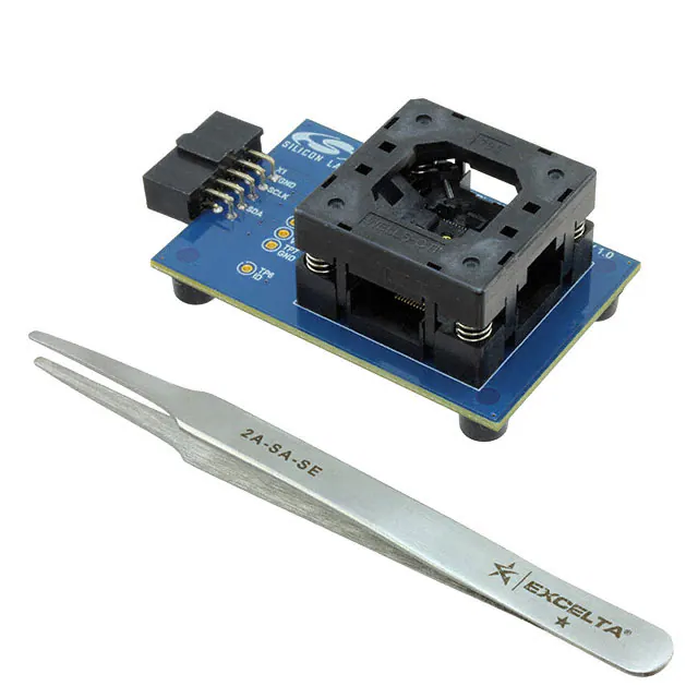
-
SI5332-40SKT-DK
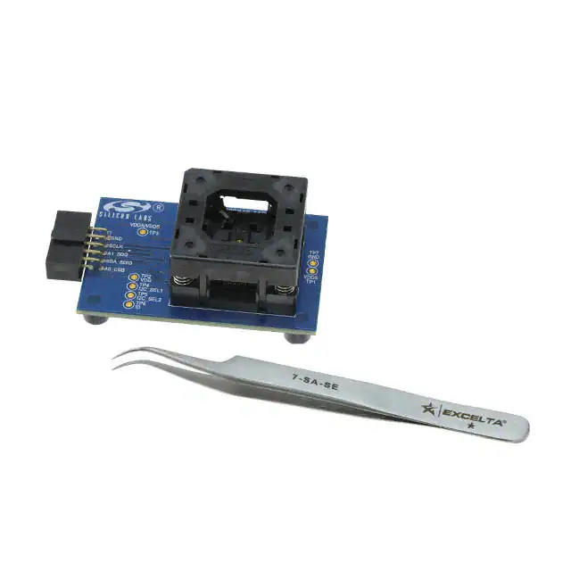
Skyworks Solutions Inc.
-
SI538X4X-64SKT-DK
Skyworks Solutions Inc.
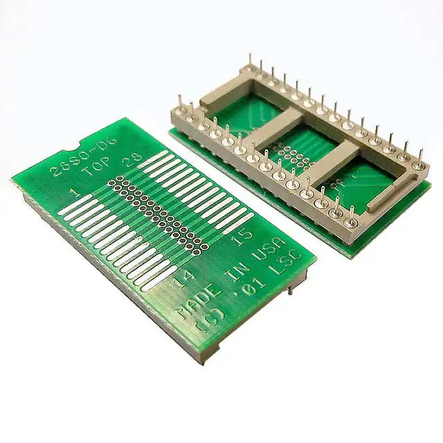
-
PA-SOD6SM18-28
Logical Systems Inc.
-
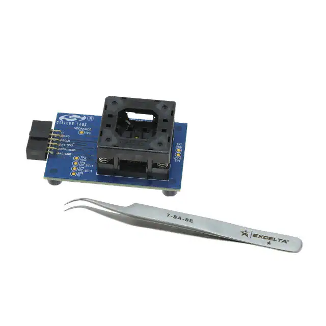
SI538X4X-44SKT-DK
Skyworks Solutions Inc.

-
SLG47528V-SKT
Renesas Electronics Operations Services Limited
-
SLG47525V-SKT
Renesas Electronics Operations Services Limited
-
LSOCTS08EA-1
BPM Microsystems
-
ATSTK600-UC3A0X-144
Microchip Technology
-
LSOCS08EA-1
BPM Microsystems
Tech Hub

A practical engineering and sourcing framework covering lifecycle verification, lifetime-buy calculations, replacement qualification, supplier checks and counterfeit-risk controls.

TTL and CMOS logic families differ in thresholds, loading, output drive, power and timing. This engineering guide compares 74HC and 74HCT, calculates noise margins and checks 3.3 V/5 V compatibility.

A practical engineering guide to 3.3V and 5V logic compatibility, input thresholds, resistor dividers, translator ICs, MOSFET level shifting, I2C pull-ups, timing limits and power-sequencing risks.

The 74HC595 uses push-pull logic outputs, while the TPIC6B595 uses 50 V open-drain DMOS sinks for higher-power loads. This guide compares timing, current limits, 3.3 V interfacing, load wiring, thermal…

The 74HC595 converts serial data into eight stable parallel outputs. This guide covers pin functions, shift and storage timing, OE and MR behavior, drive-current limits, cascading, voltage compatibilit…

A technical comparison of level-sensitive latches and edge-triggered flip-flops, covering timing windows, setup and hold limits, master–slave operation, time borrowing, race-through, HDL inference and…

A D latch stores one bit while Enable controls when data can pass. This reference covers gate-level operation, truth tables, transparency, setup and hold timing, LE versus OE, common ICs and practical …

An SR latch stores one bit through cross-coupled feedback. This engineering reference covers NOR and NAND implementations, truth tables, forbidden-state recovery, gated operation, switch debouncing, fa…

Latch circuits retain one bit through feedback. This technical reference covers SR and D latches, truth tables, transparency, timing limits, latch-versus-flip-flop behavior, applications and common log…

An engineering guide to LED driver operation, constant-current and constant-voltage outputs, linear and switching topologies, dimming, IC selection, calculations, replacement compatibility, and fault c…


