
 My Inquiry
 My Account


Renesas SLG55594V

- Part No.:
- SLG55594V
- Manufacturer:
- Renesas
- Category:
- Analog Switches - Special Purpose
- Package:
- 8-WFDFN Exposed Pad
- Datasheet:
-
 SLG55594V.pdf
- Description:
- USB HOST CHARGER IDENTIFICATION
- Quantity:
- Payment:

- Shipping:

Inventory:2,476
Please send an inquiry. Send us your inquiry, and we will respond immediately.
Product details
Overview
SLG55594V from Silego Technology is a USB host charger identification IC with integrated high-speed analog switches for D+/D− signal routing. It supports USB Battery Charging Specification Rev 1.2 (including data contact detection), Apple-compliant resistor biasing, legacy D+/D− short detection, and CDP mode enabling 1.5A charging with active USB 2.0 data communication. Used in smartphone docking stations and portable USB hubs requiring intelligent charging handshaking.
For engineers reviewing the SLG55594V datasheet, SLG55594V pinout, SLG55594V application, or SLG55594V equivalent, this page delivers verified technical context, real-world design meaning of key specs, validated pin functions, and confirmed alternative options for USB charger ID and switch integration in consumer electronics power management systems.
Technical Context
The SLG55594V implements dual-path USB 2.0 analog switching (TDP/TDM ↔ DP/DM) with 4.0 Ω typical on-resistance and 4.0 pF typical on-capacitance to preserve signal integrity up to 480 Mbps. Its internal FSM performs automatic charger classification across DCP, SDP, and CDP modes using programmable resistor dividers and voltage comparators referenced to VREF1/VREF2.
Charging mode selection is controlled by CB and SMART-CDP inputs: CB = 0 enables autodetection with mouse/keyboard wake-up from S3; CB = 1 + SMART-CDP = 1 activates CDP mode with 1.5A current support and live data path. The CEN# open-drain output pulses high for 2 s (typ) to control external current-limit switches during mode transitions.
Key Specifications
| Parameter | Value and Actual Design Meaning |
|---|---|
| Supply Range | 4.5 V to 5.5 V - compatible with standard USB VBUS without LDO; requires 0.1 μF local decoupling. |
| On Resistance (TDP/TDM) | 4.0 Ω typ - ensures minimal voltage drop and power loss during 1.5A CDP charging. |
| On Capacitance (DP/DM) | 4.0 pF typ - maintains USB 2.0 high-speed eye diagram integrity and meets ≤10 ps jitter budget. |
| CDP Mode Support | Yes - enables simultaneous 480 Mbps data transfer and 1.5A charging per BC1.2 Rev 1.2. |
| ESD Protection (DP/DM) | ±8 kV HBM - protects exposed USB connector lines against common handling and system-level ESD events. |
| Operating Temp | –40 °C to +85 °C - qualified for consumer portable device ambient environments including battery-powered enclosures. |
Pinout & Package
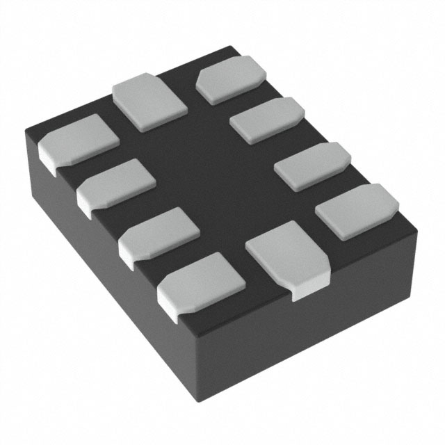
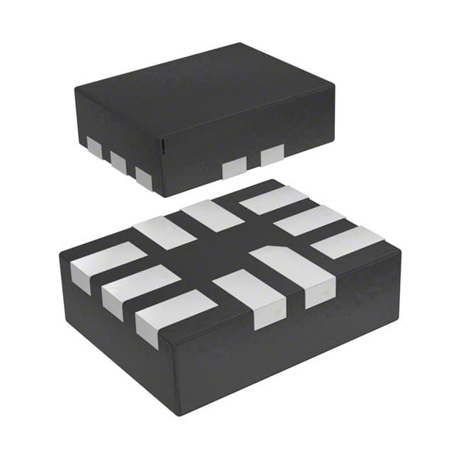
TDFN-8 package (2.0 mm × 2.0 mm × 0.75 mm), thermal pad connected to GND for thermal dissipation and noise reduction. JEDEC MO-229 WCCD compliant.
| Pin/Terminal | Circuit Role | Design Meaning |
|---|---|---|
| 1 CEN# | P-FET open-drain output | Active-high 2 s pulse to enable external current-limit switch during charger mode transition. |
| 2 DM | USB connector D− I/O | Direct connection to downstream USB device D− line; routed through internal switch to TDM. |
| 3 DP | USB connector D+ I/O | Direct connection to downstream USB device D+ line; routed through internal switch to TDP. |
| 4 SMART-CDP | Digital control input | Selects CDP vs SDP behavior when CB = 1; logic high enables CDP handshake with data path active. |
| 5 VDD | Power supply input | 4.5–5.5 V supply; must be decoupled with 0.1 μF capacitor placed adjacent to pin. |
| 6 TDP | Host transceiver D+ I/O | Connects to upstream USB host controller D+; bidirectional signal path through analog switch. |
| 7 TDM | Host transceiver D− I/O | Connects to upstream USB host controller D−; bidirectional signal path through analog switch. |
| 8 CB | Digital control input | 0 = auto-detect charger type with S3 wake-up; 1 = force CDP/SDP mode based on SMART-CDP state. |
Key Features
| Feature | Design Value |
|---|---|
| USB BC1.2 Rev 1.2 compliance | Fully implements DCP detection, data contact detection, and CDP handshake - eliminates need for external microcontroller-based ID logic. |
| Apple and Samsung charge scheme support | Integrated resistor networks match Apple's 56 kΩ D+/D− bias and Samsung Galaxy Tab's specific voltage thresholds - no external resistors required. |
| Low on-resistance flatness (0.5 Ω typ) | Ensures matched rise/fall times between DP and DM paths, preserving USB differential skew <40 ps for reliable high-speed signaling. |
| SMART-CDP logic mode control | Enables "Always Data Communication" behavior: when CB = 1 and SMART-CDP = 1, device defaults to CDP if supported, falls back to SDP otherwise - simplifies firmware logic. |
| YD/T 1591-2009 compliance | Meets Chinese Telecom Standard for USB charging interface requirements - enables market access in mainland China consumer devices. |
Applications
| Smartphone Docking Station | USB-C to USB-A Adapter with Charging ID |
|---|---|
|
Use Scenario: Desktop dock connects smartphone via USB-A port while providing 1.5A charging and full USB 2.0 data sync. IC Role / Device Role / Timing Role: SLG55594V identifies host-side charger capability, configures TDP/TDM ↔ DP/DM switch path, and asserts CEN# to enable external load switch for current limiting. Use Value: Enables single-chip BC1.2-compliant charging handshaking and signal routing - reduces BOM count by eliminating discrete resistor networks and GPIO-controlled switches. |
Use Scenario: Compact adapter converts USB-C source to legacy USB-A peripheral port, supporting both fast charging and data transfer. IC Role / Device Role / Timing Role: SLG55594V acts as USB host-side charger ID engine and high-speed analog multiplexer, detecting source type (DCP/CDP/SDP) and enabling correct D+/D− path continuity. Use Value: Achieves <100 μs mode transition time and <4.0 pF channel capacitance - preserves USB 2.0 signal fidelity without equalization or re-timing. |
| Portable USB Hub with Power Delivery Negotiation | Tablet Keyboard Dock with Wake-on-USB |
|
Use Scenario: 4-port hub negotiates optimal charging current per downstream device while maintaining concurrent data throughput. IC Role / Device Role / Timing Role: SLG55594V handles per-port charger ID and switch control under MCU supervision; CEN# pulses coordinate external current-limit FET timing. Use Value: Supports dynamic CDP/SDP reconfiguration without host CPU intervention - reduces firmware complexity and improves multi-device plug-in responsiveness. |
Use Scenario: Detachable keyboard dock wakes tablet from S3 sleep state via USB mouse/keyboard activity while delivering 500 mA charging. IC Role / Device Role / Timing Role: SLG55594V monitors D+/D− for wake patterns during S3, triggers CEN# pulse to enable charging path, and routes wake signals to host controller. Use Value: Integrates wake detection, charger ID, and signal routing into one 2×2 mm package - saves PCB area versus discrete comparator + switch solution. |
Equivalent & Alternatives
The following parts are listed as comparable options for similar USB host charger identification and analog switching applications.
| Alternative Part | Technical Difference | Application Difference | Selection Advice |
|---|---|---|---|
| TPS2546RTER | Integrated USB 2.0 switch + BC1.2 ID with adjustable current limit (up to 3A); includes I²C interface for configuration. | Requires MCU I²C control; lacks native S3 wake-up support; no built-in Apple/Samsung resistor networks. | Choose when programmable current limit and telemetry are needed over fixed-function simplicity. |
| IP2721 | Dual-channel USB switch + PD sink controller; supports USB PD 3.0, BC1.2, and proprietary schemes; QFN-24 package. | Targets USB-C PD sink applications; larger footprint; higher integration but higher cost and complexity. | Choose for USB-C PD + BC1.2 hybrid systems where PD negotiation is mandatory. |
Compared with TPS2546RTER and IP2721, the SLG55594V offers minimal-footprint, zero-firmware BC1.2 compliance with native Apple/Samsung/YD/T 1591 support - ideal for cost-sensitive, space-constrained USB-A host ports where fixed-function reliability outweighs configurability.
Availability
SLG55594V is available at Aetrix Electronics and suitable for smartphone docking stations, USB-A adapters, portable hubs, and tablet keyboard docks requiring stable component supply, consistent USB charging handshaking, and high-speed signal integrity.
Supply support for SLG55594V includes scheduled delivery planning, volume procurement assistance, BOM continuity management, traceable sourcing, and lifecycle availability coordination for OEM customers, industrial embedded developers, connected-device designers, and electronics production programs.
Manufacturer
Silego Technology (acquired by Dialog Semiconductor in 2017, now part of Renesas Electronics) specialized in configurable mixed-signal ICs for power, interface, and timing applications.
The SLG55594V belongs to Silego's USB charger identification and analog switch product line, designed specifically for consumer electronics manufacturers needing compact, standards-compliant solutions for USB host-side charging intelligence and signal routing.
FAQ
What is the primary function of the SLG55594V in a USB host system?
The SLG55594V serves as a combined USB host charger identification IC and high-speed analog switch. It automatically detects connected USB chargers (DCP/CDP/SDP) per BC1.2 Rev 1.2, applies appropriate resistor biasing for Apple and Samsung devices, and routes D+/D− signals between host transceiver and downstream port. The SLG55594V enables intelligent charging decisions while preserving USB 2.0 signal integrity without external components.
How does the SLG55594V support CDP mode and what conditions trigger it?
The SLG55594V enters CDP mode when CB = 1 and SMART-CDP = 1, enabling simultaneous 480 Mbps USB 2.0 data communication and up to 1.5A charging. It verifies CDP capability via D+/D− voltage measurements and internal resistor divider ratios, then asserts CEN# to activate an external current-limit switch. If a non-CDP device is connected, SLG55594V automatically falls back to SDP mode during handshake - all handled autonomously without MCU involvement.
What is the role of the CEN# pin on the SLG55594V and how is it timed?
The CEN# pin on the SLG55594V is a P-FET open-drain output that pulses high for 2 seconds (typical) to control an external current-limit switch during charger mode transitions. It activates when CB changes state (0→1 or 1→0), ensuring safe inrush current management during D+/D− path reconfiguration. The SLG55594V drives CEN# to VDD–0.4V at 2 mA sink capability, and leakage remains below 1 μA when deasserted - critical for low-power S3 wake-up operation.
Does the SLG55594V require external resistors for USB charger identification?
No, the SLG55594V integrates all necessary resistor networks internally, including precise RP1/RP2 and RM1/RM2 dividers for BC1.2 DCP detection, Apple-compliant 56 kΩ bias, Samsung Galaxy Tab voltage thresholds, and YD/T 1591-2009 compliance. The RRP ratio is 1.5 ±0.015 and RRM is 125 kΩ ±25 kΩ - eliminating external components and layout sensitivity. This integration is confirmed in the Electrical Characteristics tables on pages 4–5 of the SLG55594V datasheet.
What package and thermal considerations apply to the SLG55594V?
The SLG55594V uses a 2.0 mm × 2.0 mm × 0.75 mm TDFN-8 package (JEDEC MO-229 WCCD) with an exposed thermal pad connected to GND. Maximum continuous power dissipation is 954 mW at TA = 25°C; junction temperature must stay below 150°C. Layout requires soldering the thermal pad to a minimum 10 mm² GND copper area with ≥4 thermal vias to maintain θJA < 80°C/W - essential for sustained 1.5A CDP operation without derating.
SLG55594V Specifications
- Product attributes
- Attribute value
- Manufacturer:
- Renesas
- Series:
- -
- Package/Case:
- 8-WFDFN Exposed Pad
- Packaging:
- Tape & Reel (TR)
- Product Status:
- Obsolete
- Applications:
- USB
- Multiplexer/Demultiplexer Circuit:
- -
- Switch Circuit:
- -
- Number of Channels:
- 2
- On-State Resistance (Max):
- 6Ohm
- Voltage - Supply, Single (V+):
- 4.5V ~ 5.5V
- Voltage - Supply, Dual (V±):
- -
- -3db Bandwidth:
- 1GHz
- Features:
- USB 2.0
- Operating Temperature:
- -40°C ~ 85°C
- Grade:
- -
- Qualification:
- -
- Mounting Type:
- Surface Mount
- Supplier Device Package:
- 8-TDFN (2x2)
SLG55594V FAQ
1.How can I place an order for SLG55594V through Aetrix?
Please submit a Request for Quotation (RFQ) for SLG55594V on Aetrix. Our sales agent will provide a competitive quotation and guide you through the order confirmation once you accept the terms.
2.Are the price and stock information for SLG55594V reliable?
The price and inventory of SLG55594V are updated periodically and may fluctuate due to market conditions. Stock and pricing data are typically refreshed every 24 hours. Quotation validity for SLG55594V is usually 5 days.
3.What payment methods are accepted for SLG55594V?
We accept Wire Transfer, PayPal, Credit Card, Western Union, MoneyGram, and Escrow for SLG55594V transactions.
Note: Certain payment methods may incur a processing fee.
4.How is shipping managed for SLG55594V?
SLG55594V orders can be shipped via leading logistics carriers, including DHL, UPS, FedEx, TNT, or Registered Mail.
Once your SLG55594V order is processed, you will receive an email with the shipment details and tracking number.
Note: Tracking information may take up to 24 hours to appear. Express delivery typically takes 3–5 business days.
5.How can I obtain technical support or documentation for SLG55594V?
For technical support, including SLG55594V datasheets, pinout diagrams, or application guidance, please contact our engineering support team. They can provide detailed documentation and assistance for your SLG55594V requirements.
6.How does Aetrix verify that SLG55594V is sourced from the original manufacturer or authorized distributors?
All SLG55594V products on Aetrix are procured from qualified distributors and authorized channels. Our dedicated quality assurance team conducts strict verification, including traceability checks and, if necessary, third-party testing. This ensures that SLG55594V meets industry standards.
7.What is the process for return or replacement of SLG55594V?
All SLG55594V units undergo pre-shipment inspection (PSI). If there is an issue with SLG55594V, returns or replacements are accepted under the following conditions:
1.Quantity discrepancies, incorrect items, or visible external defects (such as breakage or corrosion), acknowledged by Aetrix.
2.The issue is reported within 90 days of delivery.
3.The SLG55594V part is unused and in its original packaging.
Return procedure for SLG55594V:
1.Submit a request within 90 days.
2.Obtain a Return Material Authorization (RMA) from Aetrix.
SLG55594V Tags
-
TS3USB221ARSER
Texas Instruments
-
TS3USB221AQRSERQ1
Texas Instruments
-
NX3DV221GM,115
NXP Semiconductors
-
NX3DV2567GU,115
NXP Semiconductors
-
TS3USB221RSER
Texas Instruments
-
TS3USB221ERSER
Texas Instruments
-
TC7USB40MU,LF(S2E
Toshiba Semiconductor and Storage

-
TS3USB30EDGSR
Texas Instruments
-
PI3USB221AZUAEX
Diodes Incorporated
-
FSUSB42UMX
onsemi
-
CBTL01023GM,115
NXP Semiconductors
-
TS3USB30ERSWR
Texas Instruments
Tech Hub

TTL and CMOS logic families differ in thresholds, loading, output drive, power and timing. This engineering guide compares 74HC and 74HCT, calculates noise margins and checks 3.3 V/5 V compatibility.

A practical engineering guide to 3.3V and 5V logic compatibility, input thresholds, resistor dividers, translator ICs, MOSFET level shifting, I2C pull-ups, timing limits and power-sequencing risks.

The 74HC595 uses push-pull logic outputs, while the TPIC6B595 uses 50 V open-drain DMOS sinks for higher-power loads. This guide compares timing, current limits, 3.3 V interfacing, load wiring, thermal…

The 74HC595 converts serial data into eight stable parallel outputs. This guide covers pin functions, shift and storage timing, OE and MR behavior, drive-current limits, cascading, voltage compatibilit…

A technical comparison of level-sensitive latches and edge-triggered flip-flops, covering timing windows, setup and hold limits, master–slave operation, time borrowing, race-through, HDL inference and…

A D latch stores one bit while Enable controls when data can pass. This reference covers gate-level operation, truth tables, transparency, setup and hold timing, LE versus OE, common ICs and practical …

An SR latch stores one bit through cross-coupled feedback. This engineering reference covers NOR and NAND implementations, truth tables, forbidden-state recovery, gated operation, switch debouncing, fa…

Latch circuits retain one bit through feedback. This technical reference covers SR and D latches, truth tables, transparency, timing limits, latch-versus-flip-flop behavior, applications and common log…

An engineering guide to LED driver operation, constant-current and constant-voltage outputs, linear and switching topologies, dimming, IC selection, calculations, replacement compatibility, and fault c…

Operational amplifier guide covering op amp basics, feedback, ideal vs real op amps, common configurations, buffer circuits, offset, bias current, gain-bandwidth, slew rate, rail-to-rail limits and sel…


