
 My Inquiry
 My Account


Renesas SLG59H1128V
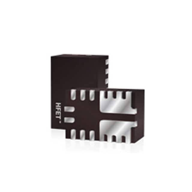
- Part No.:
- SLG59H1128V
- Manufacturer:
- Renesas
- Package:
- 18-PowerUFQFN
- Datasheet:
-
 SLG59H1128V.pdf
- Description:
- A 4.8 MM POWER CONTROL SWITCH W
- Quantity:
- Payment:

- Shipping:

Inventory:14,471
Please send an inquiry. Send us your inquiry, and we will respond immediately.
Product details
Overview
SLG59H1128V from Renesas Electronics is a high-voltage, self-powered NMOS load switch delivering 5 A continuous current with 13.1 mΩ RDSON at 22 V input, integrated VIN overvoltage lockout selection (4 thresholds), analog MOSFET current monitor output (10 µA/A), and active current limit via external RSET resistor - deployed in power-rail switching for telecom equipment and high-performance computing.
For engineers reviewing the SLG59H1128V datasheet, SLG59H1128V pinout, SLG59H1128V application, or SLG59H1128V equivalent, this page delivers verified specifications, validated 18-pin STQFN package mapping, confirmed thermal resistance (θJA = 40 °C/W), real-world SOA protection behavior (10 W threshold), and precise IOUT linearity range (0.5 A–5 A).
Technical Context
The SLG59H1128V integrates a proprietary copper-pillar interconnect NMOS FET with on-die charge pump and state-machine control logic. Its dual-stage protection combines resistor-adjustable active current limiting (2.8–3.6 A typical at RSET = 30.1 kΩ) and internal short-circuit current limit (0.5 A), while automatic SOA shutdown triggers at 10 W dissipation and folds back to 5 W during retry.
Operation spans 4.5 V–22 V input with -40 °C to +85 °C industrial temperature range. The 18-pin STQFN (1.6 × 3.0 mm) uses five fused VIN pins and five fused VOUT pins for low-inductance, high-current routing, and includes dedicated CAP pin for slew-rate control (10–20 nF) and IOUT pin with 45 µs response time to 0–2.4 A load steps.
Key Specifications
| Parameter | Value and Actual Design Meaning |
|---|---|
| Max Input Voltage | 22 V continuous; supports 20 V PoL rails with 32 V pulsed tolerance - enables use in 12 V/20 V telecom and computing systems without external clamping. |
| RDSON | 13.1 mΩ at VIN = 22 V, TA = 25 °C; stable across voltage (ΔRDSON/ΔVIN < 0.05 mΩ/V) and temperature (ΔRDSON/ΔT < 0.06 mΩ/°C) - ensures predictable conduction loss up to 5 A. |
| Continuous Current | 5 A at TJ < 150 °C; validated with θJA = 40 °C/W on 1 in² FR-4 - sustains full load in compact industrial PCB layouts with minimal heatsinking. |
| VIN OVLO Thresholds | Four pin-selectable levels: 6 V / 10.8 V / 14.4 V / 24 V (SEL[1,0] = [0,0] to [1,1]); 2% hysteresis - allows precise rail protection matching system-level voltage tolerances. |
| IOUT Monitor Accuracy | 10 µA/A typical (9.3–11 µA/A min/max) with 0.5–4 V compliance; linear from 0.5 A to 5 A - enables direct ADC interfacing for real-time load current telemetry. |
| Active Current Limit | Adjustable 1–5 A via 18–91 kΩ RSET; 3.2 A typical at 30.1 kΩ; 120 µs response - provides programmable fault containment without sacrificing startup speed. |
| SOA Protection | 10 W fixed threshold with automatic 160 ms retry and 5 W foldback - prevents thermal runaway during heavy capacitive loads or short circuits. |
Pinout & Package
SLG59H1128V is housed in a RoHS-compliant, 1.6 × 3.0 mm STQFN package with 0.40 mm pitch and 18 terminals. Thermal performance is optimized via copper pillar interconnects and fused power pins.
| Pin/Terminal | Circuit Role | Design Meaning |
|---|---|---|
| 1 ON | CMOS enable input | Level-sensitive control: HIGH (>0.9 V) initiates turn-on sequence; no internal pull-down - requires MCU GPO or system controller drive. |
| 2 SEL0, 14 SEL1 | OVLO threshold select inputs | LSB/MSB pair setting one of four VIN lockout voltages; logic LOW = GND, HIGH = 10 kΩ to VLOGIC - enables field-configurable overvoltage safety. |
| 3 GND | Main ground reference | Common return for charge pump, gate driver, current limit, and state machine - must connect directly to analog/power plane with short, low-impedance trace. |
| 4–8 VIN | Power input / FET drain | Five fused pins supply IC bias and FET channel; require ≥47 µF/50 V low-ESR capacitor to GND - minimizes input ripple and sustains transient load demands. |
| 9–13 VOUT | Power output / FET source | Five fused pins deliver switched output; require ≥22 µF/50 V low-ESR capacitor to GND - stabilizes downstream rails and reduces output droop under step loads. |
| 15 FAULT | Open-drain fault indicator | Asserts LOW within 80 µs on OVLO, current limit, or overtemperature; deasserts within 180 µs after fault removal - enables immediate system-level error handling. |
| 16 CAP | Slew rate timing node | Connects to 10–20 nF ceramic capacitor to GND; sets VOUT rise time (1.4–8 ms) and slew rate (2.7–3.9 V/ms) - prevents inrush-induced faults during hot-plug events. |
| 17 IOUT | Analog current monitor output | 10 µA/A proportional output; 0.18 nF bypass recommended; 45 µs response to 0–2.4 A steps - supports precision current sensing without shunt resistors. |
| 18 RSET | Current limit programming input | Accepts 18–91 kΩ metal-film resistor; sets active current limit from 1 A to 5 A with ±15% accuracy - enables design-specific fault current tailoring. |
Key Features
| Feature | Design Value |
|---|---|
| Self-powered architecture | No external bias required: operates from VIN rail (4.5–22 V), eliminating need for auxiliary LDO or charge pump supply. |
| Capacitor-adjustable slew rate | External 10–20 nF capacitor on CAP pin controls VOUT ramp time and inrush current - eliminates need for discrete RC networks or soft-start controllers. |
| Four-level VIN OVLO selection | PIN-strapped thresholds (6 V / 10.8 V / 14.4 V / 24 V) match diverse system rail voltages - avoids firmware updates or BOM changes when reusing design across platforms. |
| Integrated SOA protection | Hardware-based 10 W power dissipation cutoff with automatic 160 ms retry and 5 W foldback - prevents thermal damage during sustained overload without software intervention. |
| Fast output discharge | 4.4 kΩ internal RDISCHRG pulls VOUT to GND within microseconds after turn-off - ensures rapid rail discharge for safe hot-swap or sequencing. |
| Low thermal resistance package | θJA = 40 °C/W on standard FR-4; validated 17 °C ΔT at 20 V/4.5 A - enables high-power operation in space-constrained industrial modules. |
Applications
| Telecom Power Distribution | High-Performance Computing |
|---|---|
|
Use Scenario: Switching 20 V point-of-load rails in 5G base station power shelves with strict inrush and fault containment requirements. IC Role / Device Role / Timing Role: Primary load switch controlling power delivery to FPGA or ASIC voltage domains; manages turn-on slew rate and monitors real-time current draw. Use Value: Prevents bus voltage collapse during hot-plug via adjustable CSLEW and detects abnormal current draw before system-level fuses blow. |
Use Scenario: Isolating GPU or AI accelerator rails in server motherboards where 12 V/20 V supplies demand fast, reliable switching and telemetry. IC Role / Device Role / Timing Role: High-current NMOS switch with integrated current monitor feeding host BMC for predictive thermal management. Use Value: Enables real-time load profiling (via IOUT) and autonomous shutdown on overcurrent - reducing need for external sense amplifiers and fault logic. |
| Multifunction Printer Power | Motor Drive Power Sequencing |
|
Use Scenario: Controlling 24 V motor and heater rails in large-format copiers where capacitive inrush and thermal stress must be managed. IC Role / Device Role / Timing Role: Load switch with programmable active current limit and SOA protection - replaces discrete FET + controller solutions. Use Value: Eliminates need for external current-sense resistors and thermal shutdown ICs; reduces BOM count and layout area by >40%. |
Use Scenario: Enabling/disabling 12 V H-bridge gate drivers in industrial servo drives, requiring controlled VOUT ramp and fault reporting. IC Role / Device Role / Timing Role: Precision-controlled power switch with FAULT signaling and fast VOUT discharge - ensures safe gate driver reset before next cycle. Use Value: Guarantees <18 µs OFF delay and <21 µs VOUT fall time, enabling tight PWM timing margins and preventing shoot-through conditions. |
Equivalent & Alternatives
The following parts are listed as comparable options for similar load switch applications.
| Alternative Part | Technical Difference | Application Difference | Selection Advice |
|---|---|---|---|
| TPS22992DRLR | Lower max VIN (5.5 V), no VIN OVLO selection, no analog IOUT - offers 1.2 mΩ RDSON but limited to ≤5.5 V rails. | Targeted at low-voltage USB/PCIe hot-swap; lacks high-voltage SOA and programmable OVLO needed for 12–20 V telecom/computing rails. | Select only for sub-6 V applications where ultra-low RDSON outweighs missing high-voltage features. |
| RTQ2132BGQW | Higher RDSON (20 mΩ), fixed 18 V OVLO, no IOUT monitor - includes reverse-current blocking and adjustable UVLO, but no SOA protection. | Designed for automotive infotainment power domains; lacks 10 W SOA foldback and analog current telemetry critical for industrial thermal management. | Prefer for automotive environments requiring reverse-current blocking, but not for telecom/computing where SOA and IOUT are mandatory. |
Compared with TPS22992DRLR and RTQ2132BGQW, the SLG59H1128V uniquely delivers 22 V operation with pin-selectable OVLO, 10 µA/A analog current monitoring, and hardware-enforced 10 W SOA protection - making it the only option meeting full specification requirements for high-voltage, telemetry-enabled industrial load switching.
Availability
SLG59H1128V is available at Aetrix Electronics and suitable for telecom equipment, high-performance computing, multifunction printers, and motor drive power sequencing requiring stable component supply, long-term industrial temperature support (-40 °C to +85 °C), and RoHS-compliant packaging.
Supply support for SLG59H1128V includes scheduled delivery planning, volume procurement assistance, BOM continuity management, traceable sourcing, and lifecycle availability coordination for OEM customers, industrial embedded developers, connected-device designers, and electronics production programs.
Manufacturer
Renesas Electronics is a global semiconductor leader specializing in microcontrollers, analog power, and connectivity solutions for industrial, automotive, and infrastructure markets.
The SLG59H1128V belongs to Renesas' High Voltage GreenFET family, engineered specifically for robust, high-current load switching in 4.5–22 V industrial systems with integrated protection and telemetry - eliminating external components while ensuring reliability under overload and thermal stress.
FAQ
What is the maximum continuous current rating for SLG59H1128V?
The SLG59H1128V supports 5 A continuous current at junction temperature below 150 °C, validated with θJA = 40 °C/W on standard FR-4 PCB. Peak pulsed current reaches 6 A for pulses under 1 ms. Derating applies above 85 °C ambient per the thermal characteristics table in the datasheet.
How does the SLG59H1128V implement VIN overvoltage lockout?
The SLG59H1128V provides four selectable VIN OVLO thresholds (6 V, 10.8 V, 14.4 V, 24 V) via SEL0 and SEL1 pins. When VIN exceeds the selected threshold, the internal state machine opens the FET and asserts FAULT within 80 µs. Hysteresis is fixed at 2% to prevent chatter near threshold.
Can SLG59H1128V monitor load current without external sense resistors?
Yes. The SLG59H1128V provides an analog current monitor output (IOUT) delivering 10 µA per ampere of MOSFET current (9.3–11 µA/A). When routed through a ground-referenced resistor (e.g., 84.5 kΩ), it generates a proportional voltage - eliminating need for shunt resistors and associated power loss.
What is the purpose of the CAP pin on SLG59H1128V?
Connected to a 10–20 nF ceramic capacitor, the CAP pin sets VOUT slew rate and total turn-on time. At 10 nF, slew rate is 2.7–3.9 V/ms and TTOTAL_ON ranges from 1.4 ms (4.5 V) to 8 ms (22 V). This prevents inrush-induced faults and enables controlled power-up into capacitive loads.
Does SLG59H1128V include thermal protection?
Yes. The SLG59H1128V incorporates thermal shutdown at 145 °C (THERMON) and restarts at 120 °C (THERMOFF). It also implements Safe Operating Area (SOA) protection that triggers at 10 W power dissipation, opening the FET and automatically retrying after 160 ms with 5 W foldback.
What package type and dimensions does SLG59H1128V use?
The SLG59H1128V uses a 1.6 × 3.0 mm STQFN package with 0.40 mm pitch and 18 terminals. It features fused VIN (pins 4–8) and VOUT (pins 9–13) for low-inductance, high-current routing, and is RoHS-compliant with moisture sensitivity level 1.
SLG59H1128V Specifications
- Product attributes
- Attribute value
- Manufacturer:
- Renesas
- Package/Case:
- 18-PowerUFQFN
- Series:
- -
- Packaging:
- Tape & Reel (TR)
- Product Status:
- Active
- Switch Type:
- General Purpose
- Number of Outputs:
- 1
- Ratio - Input:Output:
- 1:1
- Output Configuration:
- High Side
- Output Type:
- N-Channel
- Interface:
- -
- Voltage - Load:
- -
- Voltage - Supply (Vcc/Vdd):
- 4.5V ~ 22V
- Current - Output (Max):
- 5A
- Rds On (Typ):
- 13.1mOhm
- Input Type:
- CMOS
- Features:
- -
- Fault Protection:
- -
- Operating Temperature:
- -40°C ~ 85°C (TA)
- Grade:
- -
- Qualification:
- -
- Mounting Type:
- Surface Mount
- Supplier Device Package:
- 18-STQFN (1.6x3)
SLG59H1128V FAQ
1.How can I place an order for SLG59H1128V through Aetrix?
Please submit a Request for Quotation (RFQ) for SLG59H1128V on Aetrix. Our sales agent will provide a competitive quotation and guide you through the order confirmation once you accept the terms.
2.Are the price and stock information for SLG59H1128V reliable?
The price and inventory of SLG59H1128V are updated periodically and may fluctuate due to market conditions. Stock and pricing data are typically refreshed every 24 hours. Quotation validity for SLG59H1128V is usually 5 days.
3.What payment methods are accepted for SLG59H1128V?
We accept Wire Transfer, PayPal, Credit Card, Western Union, MoneyGram, and Escrow for SLG59H1128V transactions.
Note: Certain payment methods may incur a processing fee.
4.How is shipping managed for SLG59H1128V?
SLG59H1128V orders can be shipped via leading logistics carriers, including DHL, UPS, FedEx, TNT, or Registered Mail.
Once your SLG59H1128V order is processed, you will receive an email with the shipment details and tracking number.
Note: Tracking information may take up to 24 hours to appear. Express delivery typically takes 3–5 business days.
5.How can I obtain technical support or documentation for SLG59H1128V?
For technical support, including SLG59H1128V datasheets, pinout diagrams, or application guidance, please contact our engineering support team. They can provide detailed documentation and assistance for your SLG59H1128V requirements.
6.How does Aetrix verify that SLG59H1128V is sourced from the original manufacturer or authorized distributors?
All SLG59H1128V products on Aetrix are procured from qualified distributors and authorized channels. Our dedicated quality assurance team conducts strict verification, including traceability checks and, if necessary, third-party testing. This ensures that SLG59H1128V meets industry standards.
7.What is the process for return or replacement of SLG59H1128V?
All SLG59H1128V units undergo pre-shipment inspection (PSI). If there is an issue with SLG59H1128V, returns or replacements are accepted under the following conditions:
1.Quantity discrepancies, incorrect items, or visible external defects (such as breakage or corrosion), acknowledged by Aetrix.
2.The issue is reported within 90 days of delivery.
3.The SLG59H1128V part is unused and in its original packaging.
Return procedure for SLG59H1128V:
1.Submit a request within 90 days.
2.Obtain a Return Material Authorization (RMA) from Aetrix.
SLG59H1128V Tags

-
TPS22919DCKR
Texas Instruments

-
MIC2091-1YM5-TR
Microchip Technology

-
MIC2090-1YM5-TR
Microchip Technology

-
TPS22995RZFR
Texas Instruments

-
TPS22975DSGR
Texas Instruments

-
SIP32510DT-T1-GE3
Vishay Siliconix

-
ULN2003D1013TR
STMicroelectronics

-
MIC2005A-1YM5-TR
Microchip Technology

-
MIC2005A-1YM6-TR
Microchip Technology

-
TPS22916BYFPR
Texas Instruments

-
TPS22917DBVR
Texas Instruments

-
ULN2003APWR
Texas Instruments
Tech Hub

TTL and CMOS logic families differ in thresholds, loading, output drive, power and timing. This engineering guide compares 74HC and 74HCT, calculates noise margins and checks 3.3 V/5 V compatibility.

A practical engineering guide to 3.3V and 5V logic compatibility, input thresholds, resistor dividers, translator ICs, MOSFET level shifting, I2C pull-ups, timing limits and power-sequencing risks.

The 74HC595 uses push-pull logic outputs, while the TPIC6B595 uses 50 V open-drain DMOS sinks for higher-power loads. This guide compares timing, current limits, 3.3 V interfacing, load wiring, thermal…

The 74HC595 converts serial data into eight stable parallel outputs. This guide covers pin functions, shift and storage timing, OE and MR behavior, drive-current limits, cascading, voltage compatibilit…

A technical comparison of level-sensitive latches and edge-triggered flip-flops, covering timing windows, setup and hold limits, master–slave operation, time borrowing, race-through, HDL inference and…

A D latch stores one bit while Enable controls when data can pass. This reference covers gate-level operation, truth tables, transparency, setup and hold timing, LE versus OE, common ICs and practical …

An SR latch stores one bit through cross-coupled feedback. This engineering reference covers NOR and NAND implementations, truth tables, forbidden-state recovery, gated operation, switch debouncing, fa…

Latch circuits retain one bit through feedback. This technical reference covers SR and D latches, truth tables, transparency, timing limits, latch-versus-flip-flop behavior, applications and common log…

An engineering guide to LED driver operation, constant-current and constant-voltage outputs, linear and switching topologies, dimming, IC selection, calculations, replacement compatibility, and fault c…

Operational amplifier guide covering op amp basics, feedback, ideal vs real op amps, common configurations, buffer circuits, offset, bias current, gain-bandwidth, slew rate, rail-to-rail limits and sel…


