
 My Inquiry
 My Account


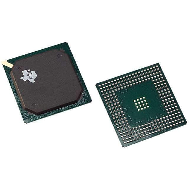
Texas Instruments SM34020AGBM32

- Part No.:
- SM34020AGBM32
- Manufacturer:
- Texas Instruments
- Category:
- DSP (Digital Signal Processors)
- Package:
- 145-BCPGA
- Datasheet:
-
 SM34020AGBM32.pdf
- Description:
- GRAPHICS SYSTEM PROCESSOR 145-CP
- Quantity:
- Payment:

- Shipping:

Inventory:4,136
Please send an inquiry. Send us your inquiry, and we will respond immediately.
Product details
Overview
SM34020AGBM32 from Texas Instruments is a radiation-hardened, second-generation 32-bit graphics system processor (GSP) designed for military and aerospace display subsystems. It features a 512-byte on-chip instruction cache, 1-μm CMOS technology, -55°C to +125°C operating range, and integrated pixel processing hardware supporting 1–32-bit pixels with raster operations. It serves as a standalone graphics engine or host-coupled CRT controller in ruggedized avionics displays.
For engineers reviewing the SM34020AGBM32 datasheet, SM34020AGBM32 pinout, SM34020AGBM32 application, or SM34020AGBM32 equivalent, key selection considerations include its 145-pin ceramic grid array package, 125-ns instruction cycle time, object-code compatibility with SMJ34010, programmable CRT timing, and direct VRAM/DRAM interface with page-mode support.
Technical Context
The SM34020AGBM32 implements a dedicated graphics architecture with hardware-accelerated XY addressing, window checking, and pixel block transfers (PIXBLT), enabling real-time raster operations without CPU intervention. Its 30 general-purpose 32-bit registers, barrel shifter, and dual register files (A/B) support both high-level language execution and optimized pixel-array manipulation.
It integrates a flexible local memory controller supporting dynamic bus sizing (16-/32-bit transfers), byte-oriented CAS strobes, and VRAM-specific functions including load write mask, block write, and serial-data-register transfers synchronized to SCLK. The coprocessor interface enables offloading of specialized compute tasks without instruction stream decoding by external logic.
Key Specifications
| Parameter | Value and Actual Design Meaning |
|---|---|
| Process Technology | 1-μm CMOS - Enables radiation-tolerant operation and stable performance across extended military temperature range. |
| Instruction Cycle Time | 125 ns - Determines maximum sustained instruction throughput of 8 MHz in real-time graphics rendering loops. |
| Address Space | 512 MB linear (32-bit) - Supports bit-addressable access to large frame buffers and texture memory in embedded display systems. |
| On-Chip Cache | 512-byte LRU instruction cache - Reduces external memory fetch latency for tight graphics kernels and interrupt service routines. |
| Pixel Processing | 1–32-bit programmable pixel size with 16 Boolean + 6 arithmetic ROPs - Enables monochrome, palette-based, and true-color rendering pipelines in single-chip solutions. |
| VRAM Interface | Direct support for 1M VRAMs with SF, TR/QE, and CAS0–CAS3 - Allows efficient block writes, color masking, and midline reloads without external glue logic. |
| Operating Temperature | -55°C to +125°C - Qualified for Class B high-reliability deployment in satellite payloads, flight control displays, and ground vehicle HUDs. |
Pinout & Package
SM34020AGBM32 is housed in a 145-pin ceramic grid array (GB) package with 17 VSS and 9 VCC pins for robust power integrity in high-noise environments. Pin assignments follow the official TI SGUS011D revision September 2004 specification.
| Pin/Terminal | Circuit Role | Design Meaning |
|---|---|---|
| LAD0–LAD31 | 32-bit multiplexed address/data bus | Carries word address (LAD4–LAD31) and status (LAD0–LAD3) at cycle start; transitions to bidirectional data path for pixel transfers and register loads. |
| RCA0–RCA12 | Multiplexed row/column address bus | Delivers DRAM row address then VRAM column address under CAMD control - enables mixed-memory topology without external address demux. |
| CAS0–CAS3 | Column address strobes | Four independent active-low strobes enable byte-selective writes to VRAM/DRAM, critical for partial-pixel updates in color planes. |
| TR/QE | Transfer/output-enable | Active-low VRAM output enable during reads; controls cycle type (block write, mask load) during special-function VRAM operations. |
| SF | Special function signal | Enables 1M VRAM block write, load write mask, and load color mask - eliminates need for discrete VRAM command sequencers. |
| ALTCH | Address latch strobe | High-to-low transition captures LAD and RCA status into external transparent latches (e.g., 54ALS373) for stable address hold during memory access. |
Key Features
| Feature | Design Value |
|---|---|
| Object-code compatibility with SMJ34010 | Enables drop-in firmware migration from first-generation GSPs without recompilation or binary modification. |
| Hardware pixel block transfer (PIXBLT) | Executes full 2D bitmap moves with clipping, transparency, and plane masking in single instruction - reduces CPU overhead in GUI compositing. |
| Programmable CRT control | Generates composite sync, separate sync, or external-sync-locked HSYNC/VSYNC - supports analog RGB, NTSC, and custom video standards. |
| Coprocessor interface with dedicated instructions | Offloads geometry transformation or compression tasks via synchronous data flow - avoids bus arbitration and instruction decode burden on host. |
| Flexible host interface with implicit addressing | Allows host processors to access full 512-MB address space using HA5–HA31 and HBS0–HBS3 - simplifies integration with PowerPC or MIL-STD-1553 host controllers. |
Applications
| Avionics Multifunction Display (MFD) | Spacecraft Telemetry Console |
|---|---|
Use Scenario: Real-time overlay of flight symbology, terrain maps, and sensor feeds onto analog RGB CRTs in fighter jet cockpits. IC Role / Device Role / Timing Role: Primary graphics engine executing PIXBLT and line-draw instructions while synchronizing to external VSYNC for flicker-free raster updates. Use Value: Hardware window checking and transparency modes eliminate software clipping overhead, enabling 60-Hz symbol refresh with <5% CPU utilization. | Use Scenario: Radiation-hardened telemetry visualization in low-Earth orbit satellites requiring continuous display of health-and-status metrics. IC Role / Device Role / Timing Role: Standalone GSP driving monochrome VRAM-based display with periodic midline reloads synchronized to SCLK for zero-latency data updates. Use Value: On-chip 512-byte instruction cache and 125-ns cycle time sustain deterministic frame generation despite single-event upsets in orbital radiation environment. |
| Ground Vehicle HUD Controller | Tactical Command Post Display |
Use Scenario: Helmet-mounted display projection system rendering augmented reality overlays onto transparent combiners in armored vehicles. IC Role / Device Role / Timing Role: Graphics co-processor interfaced to host DSP via HCS/HREAD/HWRITE, performing real-time perspective correction and alpha blending. Use Value: Programmable pixel size (1–32 bits) and arithmetic ROPs enable dynamic luminance scaling and contrast adjustment per-pixel for variable ambient lighting conditions. | Use Scenario: Ruggedized map display terminal in mobile command centers requiring simultaneous rendering of vector maps, radar blips, and text annotations. IC Role / Device Role / Timing Role: Host-coupled graphics controller managing dual-port VRAM with block writes and load color mask for rapid layer composition. Use Value: Direct VRAM support with SF and TR/QE signals reduces external logic count by 7 components, improving MTBF in field-deployable systems. |
Equivalent & Alternatives
The following parts are listed as comparable options for similar graphics system processor applications.
| Alternative Part | Technical Difference | Application Difference | Selection Advice |
|---|---|---|---|
| SMJ34010AGBM32 | First-generation GSP; lacks PIXBLT acceleration, 512-byte cache, and enhanced VRAM support; 150-ns cycle time. | Supports basic raster ops but requires software clipping and lacks transparency modes - unsuitable for real-time HUD overlays. | Select only for legacy system maintenance where SM34020AGBM32 firmware porting is impractical. |
| TMS34020GFM32 | Commercial-grade variant; same architecture but rated for -40°C to +85°C; no radiation hardening or MIL-PRF-38535 compliance. | Valid for ground-based test benches or non-flight prototypes; cannot be used in certified flight hardware or space missions. | Choose for cost-sensitive development platforms where environmental qualification is not required. |
Compared with SMJ34010AGBM32, SM34020AGBM32 delivers 20% faster instruction throughput and hardware-accelerated pixel operations essential for modern avionics symbology. Against TMS34020GFM32, it provides guaranteed operation under extreme thermal stress and ionizing radiation - critical for mission-critical display integrity.
Availability
SM34020AGBM32 is available at Aetrix Electronics and suitable for avionics MFDs, spacecraft telemetry consoles, ground vehicle HUDs, tactical command post displays, and radiation-hardened industrial HMIs requiring stable component supply over extended product lifecycles.
Supply support for SM34020AGBM32 includes scheduled delivery planning, volume procurement assistance, BOM continuity management, traceable sourcing, and lifecycle availability coordination for OEM customers, industrial embedded developers, connected-device designers, and electronics production programs.
Manufacturer
Texas Instruments is a U.S.-based semiconductor manufacturer specializing in high-reliability analog and embedded processing solutions for defense, aerospace, and industrial markets.
The SM34020A product line was developed to provide radiation-tolerant, high-performance graphics processing for mission-critical display systems where deterministic timing, long-term obsolescence mitigation, and MIL-STD compliance are mandatory.
FAQ
What is the primary function of the SM34020AGBM32 in a display system?
The SM34020AGBM32 serves as a dedicated graphics system processor that executes pixel-level raster operations-including PIXBLT, window checking, transparency, and arithmetic ROPs-without host CPU involvement. It directly drives CRT interfaces and manages VRAM/DRAM frame buffers, making it the core rendering engine in ruggedized avionics and space displays. Its architecture is optimized for deterministic, low-latency graphics updates in safety-critical environments.
Does the SM34020AGBM32 support modern digital display interfaces like LVDS or HDMI?
No. The SM34020AGBM32 was designed in the early 1990s for analog CRT systems and provides native support only for composite sync, separate sync, and externally synchronized HSYNC/VSYNC outputs. It does not include digital video transmitters, serializer/deserializer blocks, or pixel clock generators compatible with LVDS, HDMI, or DisplayPort standards. Integration with modern panels requires external video DACs and timing converters.
How does the SM34020AGBM32 handle memory refresh for DRAM-based frame buffers?
The SM34020AGBM32 includes autonomous DRAM refresh circuitry triggered by internal timers. It asserts RAS periodically while holding CAS inactive, using the RCA0–RCA12 bus to cycle through row addresses. Refresh priority is managed via the R0/R1 bus request lines: high-priority requests (e.g., >12 pending cycles) force immediate arbitration grant via GI, ensuring no frame buffer corruption occurs during intensive pixel operations.
Can the SM34020AGBM32 operate without an external host processor?
Yes. The SM34020AGBM32 can function as a fully autonomous graphics controller. When HCS is held high during RESET, it enters halted mode; writing 0 to the HLT bit in HSTCTLL releases it to execute from internal ROM or external boot PROM. Its on-chip instruction cache, 30 general-purpose registers, and programmable CRT timing allow self-contained initialization and real-time rendering without host supervision.
What packaging and thermal specifications apply to the SM34020AGBM32?
The SM34020AGBM32 uses a 145-pin ceramic grid array (GB) package with 17 ground and 9 power pins for EMI resilience. It is qualified to MIL-PRF-38535 Class B standards, operating continuously from -55°C to +125°C with full parameter testing. Thermal resistance (θJA) is 22°C/W typical; derating curves require ≤1.2 W total power dissipation above 85°C ambient to maintain reliability in sealed chassis.
SM34020AGBM32 Specifications
- Product attributes
- Attribute value
- Manufacturer:
- Texas Instruments
- Series:
- -
- Package/Case:
- 145-BCPGA
- Packaging:
- Tube
- Product Status:
- Active
- Type:
- Graphics Processor
- Interface:
- Host Interface, Multi-Processor
- Clock Rate:
- 32MHz
- Non-Volatile Memory:
- -
- On-Chip RAM:
- 1MB
- Voltage - I/O:
- 5V
- Voltage - Core:
- -
- Operating Temperature:
- -55°C ~ 125°C (TC)
- Grade:
- -
- Qualification:
- -
- Mounting Type:
- Through Hole
- Supplier Device Package:
- 145-CPGA (39.75x39.75)
SM34020AGBM32 FAQ
1.How can I place an order for SM34020AGBM32 through Aetrix?
Please submit a Request for Quotation (RFQ) for SM34020AGBM32 on Aetrix. Our sales agent will provide a competitive quotation and guide you through the order confirmation once you accept the terms.
2.Are the price and stock information for SM34020AGBM32 reliable?
The price and inventory of SM34020AGBM32 are updated periodically and may fluctuate due to market conditions. Stock and pricing data are typically refreshed every 24 hours. Quotation validity for SM34020AGBM32 is usually 5 days.
3.What payment methods are accepted for SM34020AGBM32?
We accept Wire Transfer, PayPal, Credit Card, Western Union, MoneyGram, and Escrow for SM34020AGBM32 transactions.
Note: Certain payment methods may incur a processing fee.
4.How is shipping managed for SM34020AGBM32?
SM34020AGBM32 orders can be shipped via leading logistics carriers, including DHL, UPS, FedEx, TNT, or Registered Mail.
Once your SM34020AGBM32 order is processed, you will receive an email with the shipment details and tracking number.
Note: Tracking information may take up to 24 hours to appear. Express delivery typically takes 3–5 business days.
5.How can I obtain technical support or documentation for SM34020AGBM32?
For technical support, including SM34020AGBM32 datasheets, pinout diagrams, or application guidance, please contact our engineering support team. They can provide detailed documentation and assistance for your SM34020AGBM32 requirements.
6.How does Aetrix verify that SM34020AGBM32 is sourced from the original manufacturer or authorized distributors?
All SM34020AGBM32 products on Aetrix are procured from qualified distributors and authorized channels. Our dedicated quality assurance team conducts strict verification, including traceability checks and, if necessary, third-party testing. This ensures that SM34020AGBM32 meets industry standards.
7.What is the process for return or replacement of SM34020AGBM32?
All SM34020AGBM32 units undergo pre-shipment inspection (PSI). If there is an issue with SM34020AGBM32, returns or replacements are accepted under the following conditions:
1.Quantity discrepancies, incorrect items, or visible external defects (such as breakage or corrosion), acknowledged by Aetrix.
2.The issue is reported within 90 days of delivery.
3.The SM34020AGBM32 part is unused and in its original packaging.
Return procedure for SM34020AGBM32:
1.Submit a request within 90 days.
2.Obtain a Return Material Authorization (RMA) from Aetrix.
SM34020AGBM32 Tags
-
TMS320C5535AZAY10
Texas Instruments
-
TMS320VC5501PGF300
Texas Instruments
-
ADSP-BF592KCPZ
Analog Devices Inc.
-
ADAU1463WBCPZ150
Analog Devices Inc.

-
TMS320VC5402PGE100
Texas Instruments

-
ADAU1701JSTZ-RL
Analog Devices Inc.
-
ADAU1701JSTZ
Analog Devices Inc.
-
TMS320VC5502PGF300
Texas Instruments
-
ADAU1462WBCPZ300RL
Analog Devices Inc.
-
ADAU1452KCPZRL
Analog Devices Inc.
-
ADAU1452WBCPZ-RL
Analog Devices Inc.
-
TMS320C6747DZKB3
Texas Instruments
Tech Hub

A practical engineering guide to 3.3V and 5V logic compatibility, input thresholds, resistor dividers, translator ICs, MOSFET level shifting, I2C pull-ups, timing limits and power-sequencing risks.

The 74HC595 uses push-pull logic outputs, while the TPIC6B595 uses 50 V open-drain DMOS sinks for higher-power loads. This guide compares timing, current limits, 3.3 V interfacing, load wiring, thermal…

The 74HC595 converts serial data into eight stable parallel outputs. This guide covers pin functions, shift and storage timing, OE and MR behavior, drive-current limits, cascading, voltage compatibilit…

A technical comparison of level-sensitive latches and edge-triggered flip-flops, covering timing windows, setup and hold limits, master–slave operation, time borrowing, race-through, HDL inference and…

A D latch stores one bit while Enable controls when data can pass. This reference covers gate-level operation, truth tables, transparency, setup and hold timing, LE versus OE, common ICs and practical …

An SR latch stores one bit through cross-coupled feedback. This engineering reference covers NOR and NAND implementations, truth tables, forbidden-state recovery, gated operation, switch debouncing, fa…

Latch circuits retain one bit through feedback. This technical reference covers SR and D latches, truth tables, transparency, timing limits, latch-versus-flip-flop behavior, applications and common log…

An engineering guide to LED driver operation, constant-current and constant-voltage outputs, linear and switching topologies, dimming, IC selection, calculations, replacement compatibility, and fault c…

Operational amplifier guide covering op amp basics, feedback, ideal vs real op amps, common configurations, buffer circuits, offset, bias current, gain-bandwidth, slew rate, rail-to-rail limits and sel…

Jumper cables guide covering safe connection order, red and black clamp placement, final ground connection, cable gauge, length, clamp quality, copper vs CCA cables, jump starter comparison and battery…


