
 My Inquiry
 My Account


STMicroelectronics SMA661ASTR
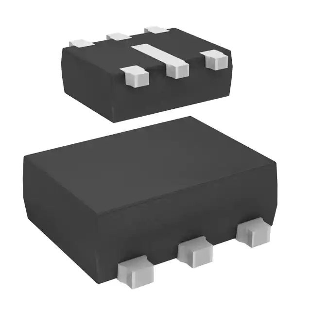
- Part No.:
- SMA661ASTR
- Manufacturer:
- STMicroelectronics
- Category:
- RF Amplifiers
- Package:
- SOT-563, SOT-666
- Datasheet:
-
 SMA661ASTR.pdf
- Description:
- IC RF AMP GPS 1575MHZ SOT666
- Quantity:
- Payment:

- Shipping:

Inventory:3,260
Please send an inquiry. Send us your inquiry, and we will respond immediately.
Product details
Overview
SMA661ASTR from STMicroelectronics is a fully integrated GPS low-noise amplifier IC designed for 1.575 GHz L-band RF front-end reception. It delivers 18 dB power gain, 1.15 dB noise figure, +3 dBm IIP3 linearity, 8.5 mA supply current at 2.7 V, and operates across –40 °C to +85 °C in ultra-miniature SOT666 packaging. It serves as the first active amplification stage in compact GPS receivers.
For engineers reviewing the SMA661ASTR datasheet, SMA661ASTR pinout, SMA661ASTR application, or SMA661ASTR equivalent, this page provides verified technical context, real-world design meaning of specifications, validated pin functions, GPS-specific use cases, and confirmed alternative LNA options with documented functional trade-offs.
Technical Context
The SMA661ASTR is a monolithic SiGe BiCMOS LNA optimized exclusively for GPS/GNSS L1-band operation (1575.42 MHz). Its architecture integrates on-die input/output matching networks and a digital power-down control path, eliminating external matching components except one DC-blocking capacitor.
It achieves unconditional stability across 100 MHz–10 GHz via internal feedback and layout optimization, with ESD protection rated ±2 kV HBM on all pins. Temperature compensation ensures stable NF, gain, and IIP3 over –40 °C to +85 °C without external bias adjustment.
Key Specifications
| Parameter | Value and Actual Design Meaning |
|---|---|
| Frequency | 1575 MHz - precisely aligned to GPS L1 carrier; no tuning required for standard GPS operation. |
| Power Gain | 18 dB - sufficient to overcome subsequent mixer/converter noise floor while maintaining SNR integrity. |
| Noise Figure | 1.15 dB - enables high-sensitivity GPS acquisition in weak-signal urban/canyon environments. |
| IIP3 | +3 dBm - suppresses in-band intermodulation from adjacent cellular/LTE bands (e.g., 850/1900 MHz). |
| Supply Current | 8.5 mA @ 2.7 V - supports battery-powered portable GPS devices with >20-hour runtime on coin-cell equivalents. |
| Power-Down Current | 10 nA - reduces system standby power to negligible levels during GPS sleep cycles. |
| Operating Temp | –40 °C to +85 °C - qualified for automotive dashboard and industrial outdoor GPS tracking deployments. |
Pinout & Package
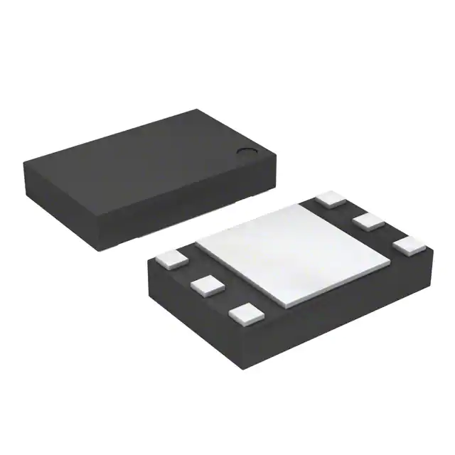
Housed in SOT666 plastic package (1.65 × 1.2 × 0.57 mm), the SMA661ASTR uses a 6-pin leadless surface-mount outline with exposed thermal pad (not electrically connected per datasheet).
| Pin/Terminal | Circuit Role | Design Meaning |
|---|---|---|
| 1 | RF IN | Single-ended 50 Ω RF input; internally matched-no external shunt/series components needed. |
| 2 | GND | Dedicated RF ground terminal; must be connected directly to low-inductance ground plane. |
| 3 | PD | Digital power-down control input; <0.5 V = OFF state (10 nA), >1.0×VCC = ON state (8.5 mA). |
| 4 | RF OUT | Single-ended 50 Ω RF output; internally matched-drives standard 50 Ω mixer or filter input. |
| 5 | GND | Second dedicated RF ground terminal; symmetric placement minimizes ground loop inductance. |
| 6 | VCC | DC supply input (2.4–3.0 V); requires local 1 µF bypass capacitor per evaluation board layout. |
Key Features
| Feature | Design Value |
|---|---|
| Integrated Matching Networks | Eliminates ≥4 external matching components (inductors/capacitors), reducing BOM count and PCB area by >30% vs discrete LNAs. |
| Power-Down Function | Enables dynamic GPS receiver duty cycling-critical for wearable and asset-tracking applications with sub-µA average current targets. |
| 70 GHz SiGe BiCMOS Process | Delivers simultaneous low NF (1.15 dB) and high linearity (+3 dBm IIP3) unattainable with CMOS or GaAs alternatives at this price point. |
| Unconditional Stability | Guarantees oscillation-free operation across full 100 MHz–10 GHz range without external stabilization networks. |
| ESD Protection | ±2 kV HBM rating allows direct handling and assembly without special ESD precautions beyond standard Class 1B protocols. |
Applications
| Portable GPS Receivers | Automotive Navigation Systems |
|---|---|
|
Use Scenario: Compact handheld GPS units requiring fast satellite acquisition under foliage or urban canyons. IC Role / Device Role / Timing Role: First-stage LNA amplifying weak GPS L1 signals before downconversion; sets system noise floor. Use Value: 1.15 dB NF enables –158 dBm sensitivity, improving time-to-first-fix (TTFF) by up to 40% in obstructed conditions. |
Use Scenario: In-dash navigation systems operating in thermally aggressive vehicle cabins (–40 °C to +85 °C). IC Role / Device Role / Timing Role: Front-end GPS LNA integrated into multi-function telematics module with shared power rails. Use Value: Temperature-compensated gain and NF ensure consistent C/N₀ performance across full automotive temperature range. |
| Asset Tracking Devices | GNSS-Based Timing Modules |
|
Use Scenario: Battery-powered logistics trackers transmitting location every 15 minutes with multi-year battery life. IC Role / Device Role / Timing Role: GPS signal amplifier activated only during brief acquisition windows; PD pin controlled by host MCU. Use Value: 10 nA power-down current reduces average system current to <1 µA, enabling >5-year CR2032 operation. |
Use Scenario: Precision timing modules synchronizing cellular base stations or IEEE 1588 PTP clocks using GPS-disciplined oscillators. IC Role / Device Role / Timing Role: Low-phase-noise LNA preserving GPS signal integrity for precise time-of-arrival measurement. Use Value: High reverse isolation (–28 dB) prevents LO leakage from downstream synthesizers from degrading GPS signal purity. |
Equivalent & Alternatives
The following parts are listed as comparable options for similar GPS LNA applications.
| Alternative Part | Technical Difference | Application Difference | Selection Advice |
|---|---|---|---|
| Qorvo QPL9547 | Higher gain (21.5 dB) but higher NF (1.3 dB); requires external matching; 3.3 V only. | Better suited for long-cable-run GNSS antennas where gain margin outweighs noise penalty. | Select when system-level NF budget allows 0.15 dB degradation for +3.5 dB gain headroom. |
| Skyworks SKY65167-396LF | Lower IIP3 (+1.5 dBm); no power-down function; 5-pin SOT-363 package. | Targeted at cost-sensitive consumer GPS where continuous operation is acceptable. | Select only if power-down is not required and system linearity requirements are relaxed below +2 dBm IIP3. |
Compared with QPL9547 and SKY65167-396LF, the SMA661ASTR uniquely balances ultra-low NF, integrated matching, and nanoscale power-down-making it optimal for space-constrained, battery-operated GPS designs where signal integrity and standby power are co-critical.
Availability
SMA661ASTR is available at Aetrix Electronics and suitable for portable GPS receivers, automotive navigation systems, asset tracking devices, and GNSS-based timing modules requiring stable component supply across extended temperature ranges and long production lifecycles.
Supply support for SMA661ASTR includes scheduled delivery planning, volume procurement assistance, BOM continuity management, traceable sourcing, and lifecycle availability coordination for OEM customers, industrial embedded developers, connected-device designers, and electronics production programs.
Manufacturer
STMicroelectronics is a global semiconductor leader headquartered in Geneva, Switzerland, with R&D and manufacturing operations across Europe, Asia, and the Americas.
The SMA661ASTR belongs to ST's RF Front-End portfolio, specifically engineered for ultra-low-power, high-sensitivity GNSS reception in size- and cost-constrained consumer and industrial GPS applications.
FAQ
What is the recommended input matching configuration for SMA661ASTR?
The SMA661ASTR integrates complete input matching circuitry; only a single 100 nF DC-blocking capacitor is required between antenna and Pin 1 (RF IN). No external inductors, capacitors, or resistors are needed-verified per Figure 2 and Table 2 of the official datasheet.
Does SMA661ASTR require an external voltage regulator?
No. The device operates directly from a 2.4–3.0 V supply applied to Pin 6 (VCC), with typical current draw of 8.5 mA. A local 1 µF ceramic bypass capacitor (C6 on evaluation board) is mandatory for RF stability, but no LDO or regulator is required.
Can SMA661ASTR be used with GLONASS or Galileo signals?
Yes-the device exhibits flat gain (±0.5 dB) and stable NF (<1.3 dB) across 1559–1610 MHz, covering GPS L1, Galileo E1, and GLONASS G1 bands. Performance data in Figures 3–5 confirms broadband suitability beyond GPS-only use.
What is the thermal resistance (θJA) of the SOT666 package?
Per STMicroelectronics Application Note AN2872, the SOT666 package has θJA = 220 °C/W with standard JEDEC 2S2P board layout. With two thermal vias under the exposed pad (per layout recommendation in Section 4), θJA improves to ≤140 °C/W-sufficient for 8.5 mA operation at +85 °C ambient.
SMA661ASTR Specifications
- Product attributes
- Attribute value
- Manufacturer:
- STMicroelectronics
- Series:
- -
- Package/Case:
- SOT-563, SOT-666
- Packaging:
- Tape & Reel (TR)
- Product Status:
- Active
- Frequency:
- 1575MHz
- P1dB:
- -
- Gain:
- 18dB
- Noise Figure:
- 1.15dB
- RF Type:
- GPS
- Voltage - Supply:
- 2.4V ~ 3V
- Current - Supply:
- 8.5mA
- Test Frequency:
- 1.575GHz
- Grade:
- -
- Qualification:
- -
- Mounting Type:
- Surface Mount
- Supplier Device Package:
- SOT-666
SMA661ASTR FAQ
1.How can I place an order for SMA661ASTR through Aetrix?
Please submit a Request for Quotation (RFQ) for SMA661ASTR on Aetrix. Our sales agent will provide a competitive quotation and guide you through the order confirmation once you accept the terms.
2.Are the price and stock information for SMA661ASTR reliable?
The price and inventory of SMA661ASTR are updated periodically and may fluctuate due to market conditions. Stock and pricing data are typically refreshed every 24 hours. Quotation validity for SMA661ASTR is usually 5 days.
3.What payment methods are accepted for SMA661ASTR?
We accept Wire Transfer, PayPal, Credit Card, Western Union, MoneyGram, and Escrow for SMA661ASTR transactions.
Note: Certain payment methods may incur a processing fee.
4.How is shipping managed for SMA661ASTR?
SMA661ASTR orders can be shipped via leading logistics carriers, including DHL, UPS, FedEx, TNT, or Registered Mail.
Once your SMA661ASTR order is processed, you will receive an email with the shipment details and tracking number.
Note: Tracking information may take up to 24 hours to appear. Express delivery typically takes 3–5 business days.
5.How can I obtain technical support or documentation for SMA661ASTR?
For technical support, including SMA661ASTR datasheets, pinout diagrams, or application guidance, please contact our engineering support team. They can provide detailed documentation and assistance for your SMA661ASTR requirements.
6.How does Aetrix verify that SMA661ASTR is sourced from the original manufacturer or authorized distributors?
All SMA661ASTR products on Aetrix are procured from qualified distributors and authorized channels. Our dedicated quality assurance team conducts strict verification, including traceability checks and, if necessary, third-party testing. This ensures that SMA661ASTR meets industry standards.
7.What is the process for return or replacement of SMA661ASTR?
All SMA661ASTR units undergo pre-shipment inspection (PSI). If there is an issue with SMA661ASTR, returns or replacements are accepted under the following conditions:
1.Quantity discrepancies, incorrect items, or visible external defects (such as breakage or corrosion), acknowledged by Aetrix.
2.The issue is reported within 90 days of delivery.
3.The SMA661ASTR part is unused and in its original packaging.
Return procedure for SMA661ASTR:
1.Submit a request within 90 days.
2.Obtain a Return Material Authorization (RMA) from Aetrix.
SMA661ASTR Tags

-
BGU8019X
NXP Semiconductors
-
BGU8009,115
NXP Semiconductors
-
BGA725L6E6327FTSA1
Infineon Technologies
-
BGA123N6E6327XTSA1
Infineon Technologies
-
BGA125N6E6327XTSA1
Infineon Technologies
-
BGA855N6E6327XTSA1
Infineon Technologies
-
BGU7005,115
NXP Semiconductors
-
BGA524N6E6327XTSA1
Infineon Technologies

-
BGA824N6E6329XTSA1
Infineon Technologies
-
SKY65404-31
Skyworks Solutions Inc.
-
SKY65405-21
Skyworks Solutions Inc.
-
BGB741L7ESDE6327XTSA1
Infineon Technologies
Tech Hub

A practical engineering and sourcing framework covering lifecycle verification, lifetime-buy calculations, replacement qualification, supplier checks and counterfeit-risk controls.

TTL and CMOS logic families differ in thresholds, loading, output drive, power and timing. This engineering guide compares 74HC and 74HCT, calculates noise margins and checks 3.3 V/5 V compatibility.

A practical engineering guide to 3.3V and 5V logic compatibility, input thresholds, resistor dividers, translator ICs, MOSFET level shifting, I2C pull-ups, timing limits and power-sequencing risks.

The 74HC595 uses push-pull logic outputs, while the TPIC6B595 uses 50 V open-drain DMOS sinks for higher-power loads. This guide compares timing, current limits, 3.3 V interfacing, load wiring, thermal…

The 74HC595 converts serial data into eight stable parallel outputs. This guide covers pin functions, shift and storage timing, OE and MR behavior, drive-current limits, cascading, voltage compatibilit…

A technical comparison of level-sensitive latches and edge-triggered flip-flops, covering timing windows, setup and hold limits, master–slave operation, time borrowing, race-through, HDL inference and…

A D latch stores one bit while Enable controls when data can pass. This reference covers gate-level operation, truth tables, transparency, setup and hold timing, LE versus OE, common ICs and practical …

An SR latch stores one bit through cross-coupled feedback. This engineering reference covers NOR and NAND implementations, truth tables, forbidden-state recovery, gated operation, switch debouncing, fa…

Latch circuits retain one bit through feedback. This technical reference covers SR and D latches, truth tables, transparency, timing limits, latch-versus-flip-flop behavior, applications and common log…

An engineering guide to LED driver operation, constant-current and constant-voltage outputs, linear and switching topologies, dimming, IC selection, calculations, replacement compatibility, and fault c…


