
 My Inquiry
 My Account


Texas Instruments SMOMAPL138BGWTA3R
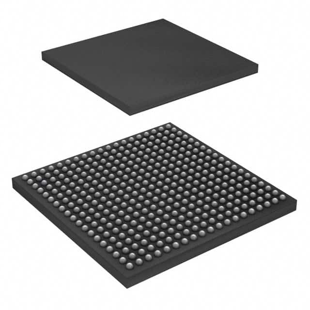
- Part No.:
- SMOMAPL138BGWTA3R
- Manufacturer:
- Texas Instruments
- Category:
- Microprocessors
- Package:
- 361-LFBGA
- Datasheet:
-
 SMOMAPL138BGWTA3R.pdf
- Description:
- IC MPU OMAP-L1X 375MHZ 361NFBGA
- Quantity:
- Payment:

- Shipping:

Inventory:2,625
Please send an inquiry. Send us your inquiry, and we will respond immediately.
Product details
Overview
SMOMAPL138BGWTA3R from Texas Instruments is a radiation-tolerant, dual-core low-power applications processor integrating a 375-MHz ARM926EJ-S RISC MPU and a 375-MHz TMS320C674x fixed/floating-point VLIW DSP on a single die. It features 32KB L1P/L1D cache, 256KB L2 unified RAM/cache, 128KB shared SRAM, DDR2/mDDR memory controller, and integrated peripherals including EMAC, USB 2.0 OTG, SATA I/II, LCD, VPIF, and PRUSS - deployed in aerospace telemetry, onboard data processing, and hardened industrial control systems.
For engineers reviewing the SMOMAPL138BGWTA3R datasheet, SMOMAPL138BGWTA3R pinout, SMOMAPL138BGWTA3R application, or SMOMAPL138BGWTA3R equivalent, key selection considerations include dual-core deterministic partitioning, radiation-hardened PBGA packaging, 1.2V core voltage at 375 MHz, EDMA3 bandwidth allocation, and peripheral coherency across ARM/DSP domains.
Technical Context
The SMOMAPL138BGWTA3R implements a tightly coupled dual-subsystem architecture: the ARM926EJ-S subsystem provides full MMU support, 16KB instruction/data caches, and Linux-capable real-time OS execution, while the C674x DSP subsystem delivers IEEE SP/DP floating-point compute with two-level cache hierarchy (32KB L1P, 32KB L1D, 256KB L2) and hardware-accelerated FFT/complex math. Both cores share access to 128KB dedicated SRAM and the 256KB L2, enabling low-latency inter-processor communication via shared memory and mailbox interrupts.
Peripherals are routed through a high-bandwidth switch fabric with configurable arbitration: the EDMA3 controller supports 64 independent channels and three transfer controllers for zero-copy data movement between DDR2, L2, McASP, McBSP, and uPP; the PRUSS provides two programmable real-time units (4KB IRAM + 512B DRAM each) for offloading time-critical I/O tasks like PWM capture, GPIO sequencing, or protocol bridging - independent of ARM/DSP scheduling.
Key Specifications
| Parameter | Value and Actual Design Meaning |
|---|---|
| Core Architecture | Dual-core SoC: 375-MHz ARM926EJ-S + 375-MHz C674x VLIW DSP - enables concurrent real-time control (ARM) and signal processing (DSP) without OS interference. |
| Memory Hierarchy | ARM: 16KB I-Cache + 16KB D-Cache + 8KB vector RAM + 64KB ROM; DSP: 32KB L1P + 32KB L1D + 256KB L2 unified RAM/cache - ensures deterministic latency for critical ISR and algorithm execution. |
| External Memory Support | 16-bit DDR2 up to 150 MHz (512 MB), 16-bit mDDR up to 133 MHz (256 MB), EMIFA for NOR/NAND/SDRAM - supports boot-from-NAND and high-throughput streaming to external storage. |
| High-Speed Interfaces | SATA I/II (1.5/3.0 Gbps), 10/100 EMAC (MII/RMII), USB 2.0 OTG + USB 1.1 OHCI - enables direct mass storage attachment, networked telemetry, and host-peripheral connectivity without bridge ICs. |
| Real-Time Peripherals | 3× eHRPWM (6 symmetric/dual-edge outputs), 3× eCAP (32-bit timestamp capture), PRUSS (2x 4KB IRAM cores), uPP (8–16-bit parallel, SDR/DDR) - meets sub-microsecond timing requirements in motor control and sensor fusion. |
| Package & Reliability | 361-ball PBGA (GWT), 0.80-mm pitch, 16 mm × 16 mm; HiRel qualification per MIL-PRF-38535 Class V - certified for operation in space-grade thermal/vacuum environments with TID tolerance ≥100 krad(Si). |
Pinout & Package
SMOMAPL138BGWTA3R is housed in a 361-ball plastic ball grid array (PBGA) package with 0.80-mm ball pitch, designated GWT suffix. The package supports 1.2-V core and 1.8-V/3.3-V I/O operation, and includes dedicated power/ground ball arrays for noise isolation between ARM, DSP, analog, and I/O domains.
| Pin/Terminal | Circuit Role | Design Meaning |
|---|---|---|
| VDD_CORE | Core Power Supply | 1.2-V nominal supply for ARM926EJ-S and C674x CPU cores - requires low-noise regulation and local decoupling to maintain timing closure at 375 MHz. |
| VDD_IO | I/O Power Supply | Configurable 1.8-V or 3.3-V supply for all general-purpose I/O banks - enables interface compatibility with legacy 3.3-V peripherals or low-power 1.8-V FPGAs. |
| CLKIN | System Clock Input | Accepts 24-MHz or 33-MHz crystal or oscillator input - feeds PLL/Clock Generator to derive ARM/DSP core clocks, DDR PHY clocks, and peripheral clocks. |
| EMU0–EMU3 | JTAG Debug Interface | Four-pin boundary-scan test and emulation interface - supports real-time debugging of both ARM and DSP cores via TI XDS560v2 or compatible emulators. |
| DDR2_DQ0–DQ15 | DDR2 Data Bus | 16-bit bidirectional data bus for DDR2 SDRAM - requires matched-length routing and on-die termination calibration for stable 150-MHz operation. |
| USB0_DP/DM | USB 2.0 OTG Differential Pair | Integrated PHY differential pair for high/full-speed OTG operation - eliminates need for external transceiver; supports device/host mode via ID pin detection. |
Key Features
| Feature | Design Value |
|---|---|
| Dual-core deterministic partitioning | ARM and DSP execute independently with separate cache hierarchies, memory maps, and interrupt controllers - prevents priority inversion and guarantees worst-case execution time for safety-critical threads. |
| EDMA3 with 64-channel arbitration | Hardware-managed DMA transfers across 12+ peripherals without CPU intervention - reduces ARM/DSP load by >70% in video capture or audio streaming workloads. |
| PRU Subsystem (PRUSS) | Two autonomous 32-bit RISC cores (4KB IRAM + 512B DRAM each) for real-time I/O offload - handles PWM generation, encoder counting, or custom protocol framing with <100-ns jitter. |
| SATA I/II native controller | On-die SATA PHY and NCQ engine supporting 32-entry command queue - enables direct connection to radiation-tolerant SSDs for onboard telemetry logging without SATA bridge IC. |
| HiRel PBGA (GWT) packaging | 361-ball 0.80-mm pitch package qualified to MIL-PRF-38535 Class V - validated for operation from –55°C to +125°C with full functionality and no parametric shift after 100 krad(Si) TID exposure. |
Applications
| Aerospace Telemetry Processing | Onboard Signal Intelligence (SIGINT) |
|---|---|
Use Scenario: Real-time preprocessing of downlinked RF sensor data on LEO satellites before compression and transmission. IC Role / Device Role / Timing Role: SMOMAPL138BGWTA3R acts as the primary signal processing node - ARM runs lightweight RTOS for task orchestration and packetization; C674x executes FFT, filtering, and demodulation kernels on raw IQ samples. Use Value: Integrated EDMA3 and L2 cache enable sustained 200+ MB/s data throughput from ADC interfaces to DDR2, eliminating external FIFO bottlenecks and reducing BOM count by 3 discrete components. |
Use Scenario: Embedded wideband spectrum analysis and emitter identification in UAV-based electronic warfare pods. IC Role / Device Role / Timing Role: SMOMAPL138BGWTA3R serves as the SIGINT front-end processor - PRUSS captures precise timestamps from RF detector pulses; C674x performs real-time spectral correlation; ARM manages database lookup and reporting. Use Value: Hardware-assisted PRUSS timestamping achieves ±2 ns resolution across 3 eCAP modules, enabling accurate time-difference-of-arrival (TDOA) calculations without software overhead. |
| Radiation-Hardened Motor Control | Hardened Industrial HMI |
Use Scenario: Closed-loop servo control in nuclear reactor instrumentation systems requiring fault-tolerant position/velocity feedback. IC Role / Device Role / Timing Role: SMOMAPL138BGWTA3R functions as the motion controller - eHRPWM generates synchronized 100-kHz gate drive signals; eCAP captures quadrature encoder edges; ARM runs safety monitor logic. Use Value: Dual-edge symmetric PWM outputs with dead-band generation ensure safe complementary FET switching; PRUSS-based encoder interpolation achieves 4× resolution boost without ARM cycle consumption. |
Use Scenario: Human-machine interface for radiation monitoring equipment in hot cells, requiring local display, touch input, and Ethernet alarm forwarding. IC Role / Device Role / Timing Role: SMOMAPL138BGWTA3R operates as the HMI controller - LCD controller drives 800×480 panel; USB OTG connects to barcode scanner; EMAC relays dose-rate alerts to plant SCADA. Use Value: Integrated LCD controller with 24-bit RGB output eliminates external timing controller; 128KB shared SRAM buffers frame buffers and touch event queues, ensuring UI responsiveness under burst network traffic. |
Equivalent & Alternatives
The following parts are listed as comparable options for similar dual-core heterogeneous processor applications.
| Alternative Part | Technical Difference | Application Difference | Selection Advice |
|---|---|---|---|
| SM320C6748BZWT | Single-core C6748 DSP (no ARM), 456 MHz, 128KB L2, no SATA/EMAC/uPP - lacks MPU-side OS support and networking stack offload capability. | Best suited for pure DSP-intensive tasks (e.g., radar beamforming) where Linux or TCP/IP is unnecessary. | Select when only floating-point signal processing is required and system-level software abstraction is handled externally. |
| AM3359BZCZ100 | ARM Cortex-A8 (1 GHz), no integrated DSP, PRU-ICSS instead of PRUSS, no SATA, DDR3 support - higher ARM performance but no native IEEE DP math or deterministic DSP pipeline. | Preferred for Linux-based HMIs or gateway applications needing rich graphics and Ethernet routing, not real-time signal processing. | Choose when application demands high-throughput ARM execution and peripheral flexibility over dual-core deterministic co-processing. |
Compared with SM320C6748BZWT and AM3359BZCZ100, SMOMAPL138BGWTA3R uniquely delivers verified radiation tolerance, integrated ARM+DSP coherency, and SATA/EMAC/uPP in a single HiRel package - making it the only option for space-qualified telemetry processors requiring simultaneous OS services and hard real-time signal analysis.
Availability
SMOMAPL138BGWTA3R is available at Aetrix Electronics and suitable for aerospace telemetry, onboard signal intelligence, and radiation-hardened motor control applications requiring stable component supply across extended mission lifetimes and obsolescence-sensitive programs.
Supply support for SMOMAPL138BGWTA3R includes scheduled delivery planning, volume procurement assistance, BOM continuity management, traceable sourcing, and lifecycle availability coordination for OEM customers, industrial embedded developers, connected-device designers, and electronics production programs.
Manufacturer
Texas Instruments is a global semiconductor company headquartered in Dallas, Texas, specializing in analog, embedded processing, and digital signal processing technologies for industrial, automotive, and aerospace markets.
The SMOMAPL138B product line was designed specifically for high-reliability embedded applications requiring radiation tolerance, deterministic dual-core processing, and integrated high-speed interfaces - targeting satellite subsystems, nuclear instrumentation, and defense electronics where failure is not an option.
FAQ
What is the maximum operating temperature range for SMOMAPL138BGWTA3R?
The SMOMAPL138BGWTA3R is qualified for operation from –55°C to +125°C ambient temperature per MIL-PRF-38535 Class V HiRel specifications. This extended range is validated across all functional blocks including ARM926EJ-S, C674x DSP, DDR2 controller, and USB PHY - with full electrical performance guaranteed at temperature extremes and after 100 krad(Si) total ionizing dose exposure.
Does SMOMAPL138BGWTA3R support boot from NAND flash?
Yes, SMOMAPL138BGWTA3R supports boot from NAND flash via its EMIFA interface with built-in BCH error correction (up to 8-bit). The internal boot ROM initializes the NAND controller, loads the first-stage bootloader (SPL) into internal RAM, and executes it - enabling field-upgradable firmware without external boot PROM or SPI flash. This capability is confirmed in Section 2.2.1 of the SLVSAQ9B datasheet.
How is cache coherency managed between the ARM926EJ-S and C674x cores in SMOMAPL138BGWTA3R?
SMOMAPL138BGWTA3R does not implement hardware cache coherency between ARM and DSP L1 caches. Coherency is maintained in software using memory barriers, cache clean/invalidate instructions (e.g., MCR p15, c7), and shared memory regions configured as non-cacheable or write-through. The 128KB shared SRAM and L2 RAM serve as coherent scratchpad zones - documented in the SMOMAPL138B Applications Processor System Reference Guide (SPRUGM7).
Can the PRUSS in SMOMAPL138BGWTA3R be used to implement custom serial protocols?
Yes, the PRUSS in SMOMAPL138BGWTA3R is explicitly designed for custom I/O protocol implementation. Each PRU core has direct access to 64 GPIO pins, supports bit-banged UART/SPI/I2C with sub-100-ns timing resolution, and can generate precise PWM waveforms or decode Manchester-encoded telemetry streams - all without ARM or DSP involvement. Example implementations are provided in TI's PRU Cookbook (SPRAC09).
What debug interfaces are available on SMOMAPL138BGWTA3R for dual-core development?
SMOMAPL138BGWTA3R provides JTAG (EMU0–EMU3) for boundary-scan and full-core debug, plus an embedded trace buffer (ETB) with 4KB capacity connected to the ARM926EJ-S ETM. The C674x DSP supports real-time trace via its own ETM port, accessible through the same JTAG chain. TI Code Composer Studio v6+ fully supports simultaneous ARM/DSP debug, breakpoint setting, and live register inspection for SMOMAPL138BGWTA3R.
SMOMAPL138BGWTA3R Specifications
- Product attributes
- Attribute value
- Manufacturer:
- Texas Instruments
- Package/Case:
- 361-LFBGA
- Series:
- OMAP-L1x
- Packaging:
- Tape & Reel (TR)
- Product Status:
- Active
- Core Processor:
- ARM926EJ-S
- Number of Cores/Bus Width:
- 1 Core, 32-Bit
- Speed:
- 375MHz
- Co-Processors/DSP:
- Signal Processing; C674x, System Control; CP15
- RAM Controllers:
- LPDDR, DDR2
- Graphics Acceleration:
- No
- Display & Interface Controllers:
- LCD
- Ethernet:
- 10/100Mbps (1)
- SATA:
- SATA 3Gbps (1)
- USB:
- USB 1.1 + PHY (1), USB 2.0 + PHY (1)
- Voltage - I/O:
- 1.8V, 3.3V
- Operating Temperature:
- -40°C ~ 105°C (TJ)
- Grade:
- -
- Qualification:
- -
- Security Features:
- Boot Security, Cryptography
- Mounting Type:
- Surface Mount
- Supplier Device Package:
- 361-NFBGA (16x16)
- Additional Interfaces:
- HPI, I2C, McASP, McBSP, MMC/SD, SPI, UART
SMOMAPL138BGWTA3R FAQ
1.How can I place an order for SMOMAPL138BGWTA3R through Aetrix?
Please submit a Request for Quotation (RFQ) for SMOMAPL138BGWTA3R on Aetrix. Our sales agent will provide a competitive quotation and guide you through the order confirmation once you accept the terms.
2.Are the price and stock information for SMOMAPL138BGWTA3R reliable?
The price and inventory of SMOMAPL138BGWTA3R are updated periodically and may fluctuate due to market conditions. Stock and pricing data are typically refreshed every 24 hours. Quotation validity for SMOMAPL138BGWTA3R is usually 5 days.
3.What payment methods are accepted for SMOMAPL138BGWTA3R?
We accept Wire Transfer, PayPal, Credit Card, Western Union, MoneyGram, and Escrow for SMOMAPL138BGWTA3R transactions.
Note: Certain payment methods may incur a processing fee.
4.How is shipping managed for SMOMAPL138BGWTA3R?
SMOMAPL138BGWTA3R orders can be shipped via leading logistics carriers, including DHL, UPS, FedEx, TNT, or Registered Mail.
Once your SMOMAPL138BGWTA3R order is processed, you will receive an email with the shipment details and tracking number.
Note: Tracking information may take up to 24 hours to appear. Express delivery typically takes 3–5 business days.
5.How can I obtain technical support or documentation for SMOMAPL138BGWTA3R?
For technical support, including SMOMAPL138BGWTA3R datasheets, pinout diagrams, or application guidance, please contact our engineering support team. They can provide detailed documentation and assistance for your SMOMAPL138BGWTA3R requirements.
6.How does Aetrix verify that SMOMAPL138BGWTA3R is sourced from the original manufacturer or authorized distributors?
All SMOMAPL138BGWTA3R products on Aetrix are procured from qualified distributors and authorized channels. Our dedicated quality assurance team conducts strict verification, including traceability checks and, if necessary, third-party testing. This ensures that SMOMAPL138BGWTA3R meets industry standards.
7.What is the process for return or replacement of SMOMAPL138BGWTA3R?
All SMOMAPL138BGWTA3R units undergo pre-shipment inspection (PSI). If there is an issue with SMOMAPL138BGWTA3R, returns or replacements are accepted under the following conditions:
1.Quantity discrepancies, incorrect items, or visible external defects (such as breakage or corrosion), acknowledged by Aetrix.
2.The issue is reported within 90 days of delivery.
3.The SMOMAPL138BGWTA3R part is unused and in its original packaging.
Return procedure for SMOMAPL138BGWTA3R:
1.Submit a request within 90 days.
2.Obtain a Return Material Authorization (RMA) from Aetrix.
SMOMAPL138BGWTA3R Tags

-
AT91SAM9260B-CU-999
Microchip Technology
-
AT91SAM9G25-CU
Microchip Technology

-
ATSAMA5D27C-CU
Microchip Technology
-
AT91SAM9X35-CU
Microchip Technology
-
AT91SAM9X25-CU
Microchip Technology

-
MCIMX6Y2CVM08AB
NXP Semiconductors
.JPG)
-
AM3352BZCZ100
Texas Instruments
-
AT91SAM9260B-CU
Microchip Technology

-
AT91SAM9260B-QU
Microchip Technology

-
ATSAMA5D31A-CU
Microchip Technology
-
AT91SAM9G20B-CU-999
Microchip Technology
-
MCIMX6Y2CVM05AB
NXP Semiconductors
Tech Hub

A practical engineering guide to 3.3V and 5V logic compatibility, input thresholds, resistor dividers, translator ICs, MOSFET level shifting, I2C pull-ups, timing limits and power-sequencing risks.

The 74HC595 uses push-pull logic outputs, while the TPIC6B595 uses 50 V open-drain DMOS sinks for higher-power loads. This guide compares timing, current limits, 3.3 V interfacing, load wiring, thermal…

The 74HC595 converts serial data into eight stable parallel outputs. This guide covers pin functions, shift and storage timing, OE and MR behavior, drive-current limits, cascading, voltage compatibilit…

A technical comparison of level-sensitive latches and edge-triggered flip-flops, covering timing windows, setup and hold limits, master–slave operation, time borrowing, race-through, HDL inference and…

A D latch stores one bit while Enable controls when data can pass. This reference covers gate-level operation, truth tables, transparency, setup and hold timing, LE versus OE, common ICs and practical …

An SR latch stores one bit through cross-coupled feedback. This engineering reference covers NOR and NAND implementations, truth tables, forbidden-state recovery, gated operation, switch debouncing, fa…

Latch circuits retain one bit through feedback. This technical reference covers SR and D latches, truth tables, transparency, timing limits, latch-versus-flip-flop behavior, applications and common log…

An engineering guide to LED driver operation, constant-current and constant-voltage outputs, linear and switching topologies, dimming, IC selection, calculations, replacement compatibility, and fault c…

Operational amplifier guide covering op amp basics, feedback, ideal vs real op amps, common configurations, buffer circuits, offset, bias current, gain-bandwidth, slew rate, rail-to-rail limits and sel…

Jumper cables guide covering safe connection order, red and black clamp placement, final ground connection, cable gauge, length, clamp quality, copper vs CCA cables, jump starter comparison and battery…


