
 My Inquiry
 My Account


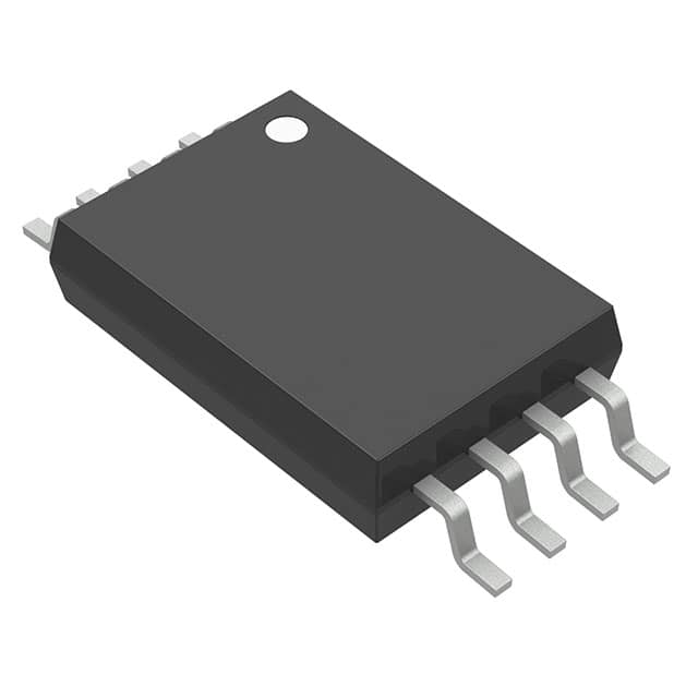
Texas Instruments SN65240PW
- Part No.:
- SN65240PW
- Manufacturer:
- Texas Instruments
- Category:
- Mixed Technology
- Package:
- 8-TSSOP (0.173", 4.40mm Width)
- Datasheet:
-
 SN65240PW.pdf
- Description:
- TVS DEVICE MIXED 7V 8-TSSOP
- Quantity:
- Payment:

- Shipping:

Inventory:2,209
Please send an inquiry. Send us your inquiry, and we will respond immediately.
Product details
Overview
SN65240PW from Texas Instruments is a quadruple unidirectional transient voltage suppressor (TVS) designed for ESD protection of USB full-speed and low-speed ports. It features 6.5-V minimum breakdown voltage, 35-pF typical input capacitance, ≤1-µA leakage at 6 V, ±15-kV HBM ESD rating, and operates from –40°C to 85°C. It protects D+ and D– data lines in USB transceivers against electrical noise transients.
For engineers reviewing the SN65240PW datasheet, SN65240PW pinout, SN65240PW application, or SN65240PW equivalent, this page delivers verified technical context, package-specific pin functions, real-world USB port protection use cases, and validated alternative options for robust I/O hardening design.
Technical Context
The SN65240PW integrates four independent unidirectional TVS diodes in a single TSSOP-8 package, each with Zener-triggered transistor-based clamping for positive transients and forward-biased diode conduction for negative transients. Its structure enables fast response to ESD events while maintaining high-impedance operation during normal USB signaling.
It operates without external power supply, relying solely on transient voltage thresholds (6.5 V min breakdown) to activate clamping. The device requires direct, low-inductance grounding via all four GND pins to ensure effective shunting of surge current-critical for preserving signal integrity at 12 Mbps USB full-speed data rates.
Key Specifications
| Parameter | Value and Actual Design Meaning |
|---|---|
| Breakdown Voltage | 6.5 V min - Ensures clamping activates above USB 5-V supply but below transceiver damage threshold. |
| Input Capacitance | 35 pF typical - Low enough to avoid signal distortion at 12 Mbps full-speed USB, unsuitable for USB 2.0 HS. |
| Leakage Current | ≤1 µA at 6 V - Minimizes standby power loss and avoids loading USB data lines during idle states. |
| ESD Rating (HBM) | ±15 kV - Exceeds IEC 61000-4-2 system-level requirements for robust human-handling immunity. |
| Operating Temp | –40°C to +85°C - Validated for industrial-grade USB host/peripheral deployment in embedded systems. |
| Package | TSSOP-8 (PW) - 3.0 mm × 4.4 mm footprint with exposed thermal pad compatibility for board-level heat dissipation. |
Pinout & Package
TSSOP-8 (PW) package: 3.00 mm × 4.40 mm body, 1.2 mm max height, lead pitch 0.65 mm, RoHS-compliant NiPdAu finish, MSL Level-1 (260°C peak reflow).
| Pin/Terminal | Circuit Role | Design Meaning |
|---|---|---|
| A | Analog input | Transient suppressor input for USB D+ line - connects directly to upstream/downstream transceiver D+. |
| B | Analog input | Transient suppressor input for USB D– line - pairs with Pin A to protect differential data path. |
| C | Analog input | Transient suppressor input for third I/O line - supports multi-port or auxiliary signal protection. |
| D | Analog input | Transient suppressor input for fourth I/O line - enables quad-channel suppression in compact layout. |
| GND (Pins 1, 3, 5, 7) | Power | Four dedicated ground terminals - mandatory connection to solid ground plane to minimize L(di/dt) during ESD events. |
Key Features
| Feature | Design Value |
|---|---|
| Quadruple unidirectional TVS | Four independent clamping paths in one TSSOP-8 package - reduces PCB area vs discrete diode arrays. |
| Low 35-pF capacitance | Preserves USB full-speed signal rise/fall times - avoids bit errors or eye diagram closure at 12 Mbps. |
| ≤1-µA leakage at 6 V | Prevents DC loading of USB data lines - maintains valid logic levels and avoids false detection in idle states. |
| ±15-kV HBM ESD rating | Validated system-level protection - meets stringent industrial and commercial USB port reliability requirements. |
| Multi-GND pin architecture | Four ground connections lower parasitic inductance - critical for diverting >9-A ESD current within <1 ns. |
Applications
| USB Full-Speed Host Port | USB Full-Speed Peripheral |
|---|---|
Use Scenario: Protecting front-panel USB Type-A ports on industrial PCs or embedded controllers exposed to frequent hot-plug cycles and operator ESD. IC Role / Device Role / Timing Role: Transient suppressor placed between connector and USB transceiver - clamps ESD spikes before they reach PHY silicon. Use Value: Enables reliable operation under ±15-kV HBM stress without degrading 12-Mbps data integrity or increasing system BOM count. | Use Scenario: Hardening USB interfaces on medical sensors or test equipment where cable disconnect/reconnect occurs in clinical or lab environments. IC Role / Device Role / Timing Role: Quad-channel TVS guarding D+, D–, VBUS sense, and ID lines - provides coordinated protection across multiple I/O paths. Use Value: Prevents latch-up or permanent damage to USB controller ASICs operating at 3.3-V or 5-V CMOS nodes. |
| USB Hub Controller Interface | Industrial USB-to-Serial Bridge |
Use Scenario: Securing downstream ports on USB 2.0 hubs used in factory automation gateways handling multiple peripheral attachments. IC Role / Device Role / Timing Role: Line-specific clamping per port - isolates transient energy on one port from affecting others via shared ground. Use Value: Maintains hub uptime and prevents cascading failure when one port receives an ESD strike during maintenance. | Use Scenario: Adding ESD resilience to RS-232/485 converters with USB upstream connectivity deployed in noisy plant-floor environments. IC Role / Device Role / Timing Role: Dual-line suppression on D+/D– plus auxiliary line protection - extends survivability beyond basic transceiver specs. Use Value: Eliminates field returns due to USB interface failure caused by electrostatic discharge during technician servicing. |
Equivalent & Alternatives
The following parts are listed as comparable options for similar transient suppression applications.
| Alternative Part | Technical Difference | Application Difference | Selection Advice |
|---|---|---|---|
| SN65240PWR | TSSOP-8, active production status, identical electrical specs and pinout, same 3.0 × 4.4 mm footprint. | Same USB full-speed protection function; differs only in tape-and-reel packaging (2000 pcs vs obsolete tube format). | Select SN65240PWR for new designs requiring guaranteed long-term availability and automated SMT assembly. |
| SN75240PW | TSSOP-8 package, same pinout, but rated for 0°C to 70°C ambient - lacks industrial temperature range. | Suitable for commercial desktop peripherals but not for extended-temperature industrial USB hosts or field-deployed peripherals. | Choose SN75240PW only if operating environment stays within 0–70°C and cost sensitivity outweighs temperature margin. |
Compared with SN65240PW, SN65240PWR offers identical performance with assured supply continuity, while SN75240PW trades industrial temp range for lower cost in benign environments - making SN65240PW the optimal choice for ruggedized USB designs requiring –40°C to 85°C operation.
Availability
SN65240PW is available at Aetrix Electronics and suitable for USB full-speed host ports, industrial peripheral interfaces, and embedded hub controller designs requiring stable component supply across extended temperature ranges and long production lifecycles.
Supply support for SN65240PW includes scheduled delivery planning, volume procurement assistance, BOM continuity management, traceable sourcing, and lifecycle availability coordination for OEM customers, industrial embedded developers, connected-device designers, and electronics production programs.
Manufacturer
Texas Instruments is a global semiconductor company delivering analog and embedded processing solutions, with leadership in precision analog, power management, and interface technologies.
The SN65240PW belongs to TI's USB transient suppressor product line, engineered specifically to harden USB 1.1 full-speed and low-speed interfaces against ESD and electrical noise in industrial, computing, and medical applications.
FAQ
What is the primary function of the SN65240PW in a USB interface?
The SN65240PW serves as a quadruple unidirectional transient voltage suppressor that protects USB D+ and D– data lines from ESD and electrical noise transients. It clamps voltage spikes above 6.5 V to prevent damage to downstream USB transceivers or ASICs. Its 35-pF capacitance and ≤1-µA leakage ensure compatibility with full-speed (12 Mbps) USB signaling without signal degradation. The SN65240PW achieves this without requiring external power, operating purely on voltage-threshold activation.
Does the SN65240PW support USB 2.0 High-Speed (480 Mbps) operation?
No, the SN65240PW does not support USB 2.0 High-Speed operation. Its 35-pF typical input capacitance is too high for 480-Mbps signaling, which demands sub-2-pF capacitance to maintain signal integrity and eye diagram compliance. The datasheet explicitly states the SN65240PW is intended for USB low-speed (1.5 Mbps) and full-speed (12 Mbps) applications only. For USB 2.0 HS, designers must select lower-capacitance TVS devices such as the TPD2EUSB30 or similar high-bandwidth suppressors.
How many ground connections does the SN65240PW require, and why are they critical?
The SN65240PW has four dedicated GND pins (Pins 1, 3, 5, and 7) in its TSSOP-8 package, and all must be connected to a low-inductance ground plane. This multi-ground architecture minimizes parasitic inductance in the surge-current path, enabling effective shunting of high-di/dt ESD transients (up to ±9 A peak). Failure to connect all GND pins degrades clamping speed and increases voltage overshoot, risking USB transceiver damage. Board layout guidelines mandate direct vias to a solid ground plane - not daisy-chained traces - to preserve the SN65240PW's ±15-kV HBM rating.
What is the significance of the 6.5-V minimum breakdown voltage for the SN65240PW?
The 6.5-V minimum breakdown voltage ensures the SN65240PW remains non-conductive during normal USB operation (where VBUS = 4.75–5.25 V and data swings are ±0.3 V), preventing signal loading or DC leakage. It activates clamping only when transients exceed this threshold - safely above the USB supply rail but well below the 7–10-V damage threshold of typical 3.3-V/5-V CMOS transceivers. This margin allows the SN65240PW to absorb energy from ±15-kV HBM strikes without interfering with legitimate signaling, making it ideal for protecting sensitive USB PHY layers.
Is the SN65240PW compatible with both 3-V and 5-V USB transceivers?
Yes, the SN65240PW is explicitly designed to protect submicron 3-V and 5-V USB transceivers. Its 6.5-V minimum breakdown voltage provides sufficient headroom above 3.3-V logic rails while remaining compatible with 5-V tolerant USB PHYs. The device's low leakage (≤1 µA at 6 V) avoids pulling down data line voltages in either voltage domain, and its unidirectional architecture ensures correct polarity alignment with USB differential signaling. TI's datasheet confirms suitability for both 3-V and 5-V circuits in the "Features" and "Description" sections of the SN65240PW documentation.
SN65240PW Specifications
- Product attributes
- Attribute value
- Manufacturer:
- Texas Instruments
- Package/Case:
- 8-TSSOP (0.173", 4.40mm Width)
- Series:
- -
- Packaging:
- Bulk
- Product Status:
- Obsolete
- Voltage - Clamping:
- 7V
- Technology:
- Mixed Technology
- Number of Circuits:
- 1
- Applications:
- USB
- Grade:
- -
- Qualification:
- -
- Mounting Type:
- Surface Mount
- Supplier Device Package:
- 8-TSSOP
SN65240PW FAQ
1.How can I place an order for SN65240PW through Aetrix?
Please submit a Request for Quotation (RFQ) for SN65240PW on Aetrix. Our sales agent will provide a competitive quotation and guide you through the order confirmation once you accept the terms.
2.Are the price and stock information for SN65240PW reliable?
The price and inventory of SN65240PW are updated periodically and may fluctuate due to market conditions. Stock and pricing data are typically refreshed every 24 hours. Quotation validity for SN65240PW is usually 5 days.
3.What payment methods are accepted for SN65240PW?
We accept Wire Transfer, PayPal, Credit Card, Western Union, MoneyGram, and Escrow for SN65240PW transactions.
Note: Certain payment methods may incur a processing fee.
4.How is shipping managed for SN65240PW?
SN65240PW orders can be shipped via leading logistics carriers, including DHL, UPS, FedEx, TNT, or Registered Mail.
Once your SN65240PW order is processed, you will receive an email with the shipment details and tracking number.
Note: Tracking information may take up to 24 hours to appear. Express delivery typically takes 3–5 business days.
5.How can I obtain technical support or documentation for SN65240PW?
For technical support, including SN65240PW datasheets, pinout diagrams, or application guidance, please contact our engineering support team. They can provide detailed documentation and assistance for your SN65240PW requirements.
6.How does Aetrix verify that SN65240PW is sourced from the original manufacturer or authorized distributors?
All SN65240PW products on Aetrix are procured from qualified distributors and authorized channels. Our dedicated quality assurance team conducts strict verification, including traceability checks and, if necessary, third-party testing. This ensures that SN65240PW meets industry standards.
7.What is the process for return or replacement of SN65240PW?
All SN65240PW units undergo pre-shipment inspection (PSI). If there is an issue with SN65240PW, returns or replacements are accepted under the following conditions:
1.Quantity discrepancies, incorrect items, or visible external defects (such as breakage or corrosion), acknowledged by Aetrix.
2.The issue is reported within 90 days of delivery.
3.The SN65240PW part is unused and in its original packaging.
Return procedure for SN65240PW:
1.Submit a request within 90 days.
2.Obtain a Return Material Authorization (RMA) from Aetrix.
SN65240PW Tags
-
ESD03A5V5R17V
Stackpole Electronics Inc
-
ESDU02A5V5R17V
Stackpole Electronics Inc
-
0603ESDA-MLP7
Eaton - Electronics Division
.jpg)
-
0603ESDA2-TR2
Eaton - Electronics Division
-
PS04LTVA1
Eaton - Electronics Division
.jpg)
-
0402ESDA-MLP1
Eaton - Electronics Division
.jpg)
-
0402ESDA-MLP7
Eaton - Electronics Division
-
TPD2S017DBVR
Texas Instruments
.jpg)
-
V2F105A150Y2EDP
KYOCERA AVX
-
82307050029
Würth Elektronik
-
NCP360SNT1G
onsemi
-
V2F118A400Y2EDP
KYOCERA AVX
Tech Hub

A practical engineering guide to 3.3V and 5V logic compatibility, input thresholds, resistor dividers, translator ICs, MOSFET level shifting, I2C pull-ups, timing limits and power-sequencing risks.

The 74HC595 uses push-pull logic outputs, while the TPIC6B595 uses 50 V open-drain DMOS sinks for higher-power loads. This guide compares timing, current limits, 3.3 V interfacing, load wiring, thermal…

The 74HC595 converts serial data into eight stable parallel outputs. This guide covers pin functions, shift and storage timing, OE and MR behavior, drive-current limits, cascading, voltage compatibilit…

A technical comparison of level-sensitive latches and edge-triggered flip-flops, covering timing windows, setup and hold limits, master–slave operation, time borrowing, race-through, HDL inference and…

A D latch stores one bit while Enable controls when data can pass. This reference covers gate-level operation, truth tables, transparency, setup and hold timing, LE versus OE, common ICs and practical …

An SR latch stores one bit through cross-coupled feedback. This engineering reference covers NOR and NAND implementations, truth tables, forbidden-state recovery, gated operation, switch debouncing, fa…

Latch circuits retain one bit through feedback. This technical reference covers SR and D latches, truth tables, transparency, timing limits, latch-versus-flip-flop behavior, applications and common log…

An engineering guide to LED driver operation, constant-current and constant-voltage outputs, linear and switching topologies, dimming, IC selection, calculations, replacement compatibility, and fault c…

Operational amplifier guide covering op amp basics, feedback, ideal vs real op amps, common configurations, buffer circuits, offset, bias current, gain-bandwidth, slew rate, rail-to-rail limits and sel…

Jumper cables guide covering safe connection order, red and black clamp placement, final ground connection, cable gauge, length, clamp quality, copper vs CCA cables, jump starter comparison and battery…


