
 My Inquiry
 My Account


Texas Instruments SN65DSI85TPAPRQ1
- Part No.:
- SN65DSI85TPAPRQ1
- Manufacturer:
- Texas Instruments
- Category:
- Specialized
- Package:
- 64-PowerTQFP
- Datasheet:
-
 SN65DSI85TPAPRQ1.pdf
- Description:
- IC INTFACE SPECIALIZED 64HTQFP
- Quantity:
- Payment:

- Shipping:

Inventory:2,262
Please send an inquiry. Send us your inquiry, and we will respond immediately.
Product details
Overview
SN65DSI85TPAPRQ1 from Texas Instruments is an AEC-Q100 Grade 2 automotive dual-channel MIPI DSI-to-LVDS bridge IC that converts 18-/24-bpp RGB666/RGB888 video streams over two D-PHY channels (up to 4 lanes/channel, 1 Gbps/lane) into dual-link LVDS output with pixel clock range 25–154 MHz. It supports WQXGA 2560×1600 @60 fps and WUXGA 1920×1200 @120 fps equivalent for infotainment displays.
For engineers reviewing the SN65DSI85TPAPRQ1 datasheet, SN65DSI85TPAPRQ1 pinout, SN65DSI85TPAPRQ1 application, or SN65DSI85TPAPRQ1 equivalent, key selection criteria include DSI lane configuration flexibility (1–4 lanes per channel), LVDS link mode (single/dual/two single-link), ULPS support, 1.8-V VCC supply, and HTQFP-64 thermal performance in –40°C to 105°C ambient.
Technical Context
The device implements a dual-channel MIPI D-PHY 1.00.00 front-end with configurable lane count per channel and decodes DSI video packets before formatting pixel data for LVDS serialization. Its internal PLL locks to either the DSI clock or external REFCLK (25–154 MHz) to generate precise LVDS pixel timing.
It features partial line buffering to absorb DSI–LVDS data rate mismatch, supports odd/even and left/right DSI channel mapping, and provides LVDS pin-order reversal and channel swap for PCB routing optimization. All LVDS outputs are fully differential with programmable swing (180–535 mV) and common-mode voltage (0.75–1.5 V).
Key Specifications
| Parameter | Value and Actual Design Meaning |
|---|---|
| Input Interface | Dual-channel MIPI DSI with up to 4 data lanes + 1 clock lane per channel, compliant with D-PHY v1.00.00 and DSI v1.02.00 |
| Output Interface | Dual-link LVDS, single-link LVDS, or two independent single-link LVDS interfaces; supports 18-bpp (RGB666) and 24-bpp (RGB888) |
| Pixel Clock Range | 25 MHz to 154 MHz - enables native timing for WQXGA (2560×1600) and WUXGA (1920×1200) panels at 60/120 fps equivalent |
| Supply Voltage | 1.8 V ±0.15 V VCC - low-voltage operation compatible with modern SoC I/O domains; includes 1.1-V VCORE regulator output |
| Operating Temp | –40°C to +105°C ambient - AEC-Q100 Grade 2 qualified for automotive head units, clusters, and rear-seat displays |
| ESD Rating | HBM ±4 kV, CDM ±1 kV - meets automotive robustness requirements for in-vehicle display interconnects |
| Power Consumption | 127–232 mA active current; 7.7–14 mA ULPS standby; 0.04–130 µA shutdown - supports dynamic power management in display subsystems |
Pinout & Package
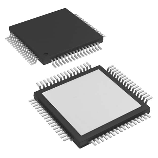
SN65DSI85TPAPRQ1 is packaged in a 64-pin HTQFP (PAP) with 10 mm × 10 mm body and 0.5-mm pitch, featuring exposed PowerPAD™ thermal pad for enhanced heat dissipation in automotive environments.
| Pin/Terminal | Circuit Role | Design Meaning |
|---|---|---|
| DA0P–DA3N, DACP/N | MIPI D-PHY Channel A inputs | Differential high-speed data/clock lanes (up to 4 data + 1 clock); support 1 Gbps/lane with LP/HS mode transition |
| DB0P–DB3N, DBCP/N | MIPI D-PHY Channel B inputs | Independent second D-PHY channel; enables dual-stream or split-panel configurations |
| A_Y0P/N–A_Y3P/N, A_CLKP/N | LVDS Channel A outputs | Four differential data lanes + clock; carry odd-pixel or left-panel data in dual-link mode |
| B_Y0P/N–B_Y3P/N, B_CLKP/N | LVDS Channel B outputs | Four differential data lanes + clock; carry even-pixel or right-panel data; supports LVDS channel swap |
| EN | Chip enable/reset input | Active-high control; asserts hardware reset when low; requires ≥10 ms hold time for reliable initialization |
| REFCLK | External LVDS pixel clock input | Optional 25–154 MHz reference; used instead of DSI clock for jitter-sensitive timing or asynchronous source sync |
| SCL/SDA, ADDR, IRQ | I²C interface and control | Local configuration bus (400 kHz); ADDR sets I²C address; IRQ signals error/status events to host processor |
Key Features
| Feature | Design Value |
|---|---|
| Dual-channel DSI receiver | Configurable for 1–4 D-PHY lanes per channel, supporting flexible bandwidth allocation between display streams |
| LVDS output flexibility | Single-link, dual-link, or two independent single-link modes - adapts to panel vendor requirements without hardware change |
| ULPS and low-power modes | Full MIPI Ultra-Low Power State support plus SHUTDOWN and reduced-swing LVDS options - cuts system power during display idle |
| LVDS routing aids | Pin-order reversal and channel swap on both LVDS links - simplifies high-density PCB layout and reduces crosstalk risk |
| Thermal design support | HTQFP-64 PowerPAD™ package with RθJA = 36.1°C/W - enables conduction cooling in sealed automotive enclosures |
Applications
| Infotainment Head Unit With Integrated Display | Hybrid Automotive Cluster |
|---|---|
Use Scenario: Central display unit driven by application processor with MIPI DSI output, directly interfacing a high-resolution TFT LCD. IC Role / Device Role / Timing Role: DSI-to-LVDS protocol and electrical bridge; provides pixel-clock synchronization, lane deskew, and format conversion. Use Value: Enables use of cost-effective LVDS panels with modern DSI-capable SoCs while maintaining 60 fps WQXGA timing integrity. |
Use Scenario: Digital instrument cluster combining analog gauges and digital graphics, requiring deterministic video latency and EMI resilience. IC Role / Device Role / Timing Role: High-reliability video interface translating DSI from MCU to dual-link LVDS driving segmented or full-TFT cluster display. Use Value: AEC-Q100 qualification and 105°C operation ensure functional safety compliance; ULPS support reduces power during vehicle sleep mode. |
| Infotainment Rear-Seat Entertainment | Industrial Human Machine Interface (HMI) |
Use Scenario: Dual-display rear-seat system where one SN65DSI85TPAPRQ1 drives left seat, another drives right seat via independent DSI channels. IC Role / Device Role / Timing Role: Dual-channel bridge operating in two single-link LVDS mode - isolates video paths for independent content rendering. Use Value: Eliminates need for separate DSI transmitters; leverages single IC for multi-display topology with minimal board space. |
Use Scenario: Factory-floor HMI panel with wide-temp TFT display, connected to industrial-grade ARM SoC with MIPI DSI output. IC Role / Device Role / Timing Role: Robust display interface handling vibration, EMI, and extended temperature cycling without frame drop or skew. Use Value: 4 kV HBM ESD rating and 20.6°C/W RθJB ensure long-term reliability in harsh industrial environments. |
Equivalent & Alternatives
The following parts are listed as comparable options for similar DSI-to-LVDS bridge applications.
| Alternative Part | Technical Difference | Application Difference | Selection Advice |
|---|---|---|---|
| SN65DSI84TPAPRQ1 | Single-channel DSI input (4-lane max), single-link LVDS only; no dual-link or two-single-link mode | Suitable for lower-resolution panels (≤WUXGA) or cost-sensitive single-display systems | Select when dual-channel DSI or dual-link LVDS capability is unnecessary - reduces BOM cost and layout complexity |
| DS90UH940NQSQEVM | FHD-optimized serializer with embedded FPD-Link III; requires companion deserializer; no native DSI support | Targets longer cable runs (>1 m) using shielded twisted pair; not a direct DSI-to-LVDS replacement | Choose for high-noise environments or when extending display interface beyond PCB traces - adds system-level complexity |
Compared with SN65DSI84TPAPRQ1, SN65DSI85TPAPRQ1 delivers dual-channel scalability and dual-link LVDS for higher-resolution panels; versus DS90UH940NQSQEVM, it offers direct DSI integration without serializer-deserializer pairing, reducing component count and latency.
Availability
SN65DSI85TPAPRQ1 is available at Aetrix Electronics and suitable for automotive infotainment head units, hybrid instrument clusters, and industrial HMIs requiring stable component supply across extended temperature ranges and long production lifecycles.
Supply support for SN65DSI85TPAPRQ1 includes scheduled delivery planning, volume procurement assistance, BOM continuity management, traceable sourcing, and lifecycle availability coordination for OEM customers, industrial embedded developers, connected-device designers, and electronics production programs.
Manufacturer
Texas Instruments is a global semiconductor leader specializing in analog, embedded processing, and automotive electronics, with decades of experience in display interface solutions and AEC-Q100-qualified components.
The SN65DSI85TPAPRQ1 belongs to TI's automotive display bridge product line, engineered specifically for MIPI DSI-to-LVDS translation in safety-critical, thermally demanding vehicle display systems.
FAQ
What is the maximum DSI data rate supported by the SN65DSI85TPAPRQ1?
The SN65DSI85TPAPRQ1 supports up to 1 Gbps per D-PHY data lane, with dual-channel configuration allowing up to 4 lanes per channel. This yields a maximum aggregate DSI input bandwidth of 8 Gbps, sufficient for 24-bpp WQXGA video at 60 fps. The device complies with MIPI D-PHY v1.00.00 and DSI v1.02.00 specifications, ensuring interoperability with standard DSI sources.
Does the SN65DSI85TPAPRQ1 require external configuration via I²C?
Yes, the SN65DSI85TPAPRQ1 requires I²C-based register initialization after power-up and reset. Critical registers-including PLL_EN (CSR 0x0D.0), SOFT_RESET (CSR 0x09.0), and LVDS format controls (e.g., CSR 0x18)-must be written in sequence before video transmission begins. The SCL/SDA pins and ADDR pin enable local configuration without host processor firmware changes.
Can the SN65DSI85TPAPRQ1 drive an 18-bpp LVDS panel?
Yes, the SN65DSI85TPAPRQ1 natively supports 18-bpp RGB666 output. When configured for 18-bpp mode, the A_Y3P/N and B_Y3P/N LVDS lanes are disabled (NC), and pixel data is mapped across the remaining three data lanes per channel. This avoids overscan or truncation issues and maintains timing alignment with legacy 18-bpp panels.
How does the SN65DSI85TPAPRQ1 handle ultra-low power state (ULPS) transitions?
The SN65DSI85TPAPRQ1 fully implements MIPI D-PHY ULPS entry and exit protocols. During ULPS, all DSI lanes enter low-power mode with controlled voltage thresholds (VIL-ULPS ≤300 mV), and the device draws only 7.7–14 mA. Exit timing adheres to D-PHY spec requirements, ensuring glitch-free resumption of high-speed video streaming without host intervention.
What thermal management provisions does the SN65DSI85TPAPRQ1 include?
The SN65DSI85TPAPRQ1 uses a 64-pin HTQFP package with integrated PowerPAD™ thermal pad, achieving RθJA = 36.1°C/W and RθJB = 20.6°C/W. For automotive applications, this allows direct thermal coupling to copper pour or heatsink, sustaining 105°C ambient operation without derating. Layout guidelines recommend minimum 4-layer board with dedicated ground/power planes and thermal vias under the PowerPAD™.
SN65DSI85TPAPRQ1 Specifications
- Product attributes
- Attribute value
- Manufacturer:
- Texas Instruments
- Series:
- -
- Package/Case:
- 64-PowerTQFP
- Packaging:
- Tape & Reel (TR)
- Product Status:
- Active
- Applications:
- -
- Interface:
- I2C
- Voltage - Supply:
- 1.65V ~ 1.95V
- Supplier Device Package:
- 64-HTQFP (10x10)
- Grade:
- Automotive
- Qualification:
- AEC-Q100
- Mounting Type:
- Surface Mount
SN65DSI85TPAPRQ1 FAQ
1.How can I place an order for SN65DSI85TPAPRQ1 through Aetrix?
Please submit a Request for Quotation (RFQ) for SN65DSI85TPAPRQ1 on Aetrix. Our sales agent will provide a competitive quotation and guide you through the order confirmation once you accept the terms.
2.Are the price and stock information for SN65DSI85TPAPRQ1 reliable?
The price and inventory of SN65DSI85TPAPRQ1 are updated periodically and may fluctuate due to market conditions. Stock and pricing data are typically refreshed every 24 hours. Quotation validity for SN65DSI85TPAPRQ1 is usually 5 days.
3.What payment methods are accepted for SN65DSI85TPAPRQ1?
We accept Wire Transfer, PayPal, Credit Card, Western Union, MoneyGram, and Escrow for SN65DSI85TPAPRQ1 transactions.
Note: Certain payment methods may incur a processing fee.
4.How is shipping managed for SN65DSI85TPAPRQ1?
SN65DSI85TPAPRQ1 orders can be shipped via leading logistics carriers, including DHL, UPS, FedEx, TNT, or Registered Mail.
Once your SN65DSI85TPAPRQ1 order is processed, you will receive an email with the shipment details and tracking number.
Note: Tracking information may take up to 24 hours to appear. Express delivery typically takes 3–5 business days.
5.How can I obtain technical support or documentation for SN65DSI85TPAPRQ1?
For technical support, including SN65DSI85TPAPRQ1 datasheets, pinout diagrams, or application guidance, please contact our engineering support team. They can provide detailed documentation and assistance for your SN65DSI85TPAPRQ1 requirements.
6.How does Aetrix verify that SN65DSI85TPAPRQ1 is sourced from the original manufacturer or authorized distributors?
All SN65DSI85TPAPRQ1 products on Aetrix are procured from qualified distributors and authorized channels. Our dedicated quality assurance team conducts strict verification, including traceability checks and, if necessary, third-party testing. This ensures that SN65DSI85TPAPRQ1 meets industry standards.
7.What is the process for return or replacement of SN65DSI85TPAPRQ1?
All SN65DSI85TPAPRQ1 units undergo pre-shipment inspection (PSI). If there is an issue with SN65DSI85TPAPRQ1, returns or replacements are accepted under the following conditions:
1.Quantity discrepancies, incorrect items, or visible external defects (such as breakage or corrosion), acknowledged by Aetrix.
2.The issue is reported within 90 days of delivery.
3.The SN65DSI85TPAPRQ1 part is unused and in its original packaging.
Return procedure for SN65DSI85TPAPRQ1:
1.Submit a request within 90 days.
2.Obtain a Return Material Authorization (RMA) from Aetrix.
SN65DSI85TPAPRQ1 Tags

-
NVT4857UKAZ
NXP Semiconductors

-
TCA8418RTWR
Texas Instruments

-
PCA9546APWR
Texas Instruments

-
MD0100N8-G
Microchip Technology

-
PCA9548APW,118
NXP Semiconductors

-
PCA9540BDP,118
NXP Semiconductors

-
PCA9548APWR
Texas Instruments

-
PCA9546APW,118
NXP Semiconductors

-
PTN3360DBS,518
NXP Semiconductors

-
PCA9546ABS,118
NXP Semiconductors

-
PCA9518PWR
Texas Instruments

-
PCA9545APW,118
NXP Semiconductors
Tech Hub

A practical engineering guide to 3.3V and 5V logic compatibility, input thresholds, resistor dividers, translator ICs, MOSFET level shifting, I2C pull-ups, timing limits and power-sequencing risks.

The 74HC595 uses push-pull logic outputs, while the TPIC6B595 uses 50 V open-drain DMOS sinks for higher-power loads. This guide compares timing, current limits, 3.3 V interfacing, load wiring, thermal…

The 74HC595 converts serial data into eight stable parallel outputs. This guide covers pin functions, shift and storage timing, OE and MR behavior, drive-current limits, cascading, voltage compatibilit…

A technical comparison of level-sensitive latches and edge-triggered flip-flops, covering timing windows, setup and hold limits, master–slave operation, time borrowing, race-through, HDL inference and…

A D latch stores one bit while Enable controls when data can pass. This reference covers gate-level operation, truth tables, transparency, setup and hold timing, LE versus OE, common ICs and practical …

An SR latch stores one bit through cross-coupled feedback. This engineering reference covers NOR and NAND implementations, truth tables, forbidden-state recovery, gated operation, switch debouncing, fa…

Latch circuits retain one bit through feedback. This technical reference covers SR and D latches, truth tables, transparency, timing limits, latch-versus-flip-flop behavior, applications and common log…

An engineering guide to LED driver operation, constant-current and constant-voltage outputs, linear and switching topologies, dimming, IC selection, calculations, replacement compatibility, and fault c…

Operational amplifier guide covering op amp basics, feedback, ideal vs real op amps, common configurations, buffer circuits, offset, bias current, gain-bandwidth, slew rate, rail-to-rail limits and sel…

Jumper cables guide covering safe connection order, red and black clamp placement, final ground connection, cable gauge, length, clamp quality, copper vs CCA cables, jump starter comparison and battery…


