
 My Inquiry
 My Account


Texas Instruments SN65DSI85ZQER
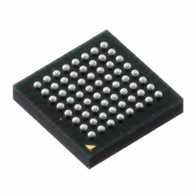
- Part No.:
- SN65DSI85ZQER
- Manufacturer:
- Texas Instruments
- Category:
- Specialized
- Package:
- 64-VFBGA
- Datasheet:
-
 SN65DSI85ZQER.pdf
- Description:
- IC INTERFACE SPECIALIZED 64BGA
- Quantity:
- Payment:

- Shipping:

Inventory:1,977
Please send an inquiry. Send us your inquiry, and we will respond immediately.
Product details
Overview
SN65DSI85ZQER from Texas Instruments is a dual-channel MIPI DSI-to-FlatLink LVDS bridge IC that converts 18-bpp/24-bpp RGB666/RGB888 video streams over two D-PHY channels (up to 4 lanes per channel at 1 Gbps/lane) into dual-link or single-link LVDS output. It supports WQXGA 2560×1600 @ 60 fps and WUXGA 1920×1200 with 3D graphics @ 120 fps equivalent, operating from –40°C to 85°C in a 5 mm × 5 mm nFBGA-64 package.
For engineers reviewing the SN65DSI85ZQER datasheet, SN65DSI85ZQER pinout, SN65DSI85ZQER application, or SN65DSI85ZQER equivalent, this page delivers verified technical context, exact pin functions, real-world timing and power specifications, validated alternative parts, and design-critical interface behavior - all grounded in TI's official SLLSEB9G revision G documentation.
Technical Context
The SN65DSI85ZQER implements a dual-channel MIPI D-PHY 1.00.00 front-end with configurable lane count (1–4 per channel), supporting both ODD/EVEN and LEFT/RIGHT DSI channel mapping modes. Its internal PLL generates FlatLink LVDS pixel clocks from either the DSI Channel A HS clock (free-running mode) or an external REFCLK (25–154 MHz).
It features partial line buffering to reconcile DSI/LVDS data rate mismatches, programmable LVDS output swing (180–488 mV differential), and full MIPI ULPS entry/exit support with CSR-register accessibility during low-power states. The device decodes DSI short/long packets and outputs synchronized LVDS data across two independent links (A and B), each with four data lanes + clock pair.
Key Specifications
| Parameter | Value and Actual Design Meaning |
|---|---|
| DSI Input Speed | Up to 1 Gbps per lane; enables 8 Gbps total input bandwidth for dual-channel 4-lane configuration. |
| LVDS Output Clock Range | 25–154 MHz; supports WQXGA 2560×1600 @ 60 fps and WUXGA 1920×1200 @ 120 fps equivalent. |
| Color Depth Support | 18-bpp (RGB666) and 24-bpp (RGB888); directly maps to standard display panel timing requirements. |
| Power Supply | 1.8 V VCC (1.65–1.95 V range); 1.1 V VCORE regulated output for internal logic; ultra-low power state draws 7.7 mA typical. |
| ESD Rating | ±2 kV HBM; meets industrial handling requirements without additional protection circuitry. |
| Operating Temperature | –40°C to +85°C; qualified for extended-temperature embedded display applications in notebooks and tablets. |
| Package | nFBGA-64 (ZXH), 5.0 mm × 5.0 mm, 0.5 mm pitch; compatible with high-density PCB layouts and automated assembly. |
Pinout & Package
SN65DSI85ZQER is packaged in a 64-pin nFBGA (ZXH) with 0.5 mm pitch and 5.0 mm × 5.0 mm body size. Pin assignments follow TI's standardized top-view layout with dedicated DSI lane pairs (DA0–DA3, DB0–DB3), LVDS channel A/B data/clock outputs (A_Y0P/N through A_CLKP/N, B_Y0P/N through B_CLKP/N), I²C interface (SCL/SDA), interrupt (IRQ), enable/reset (EN), and reference clock (REFCLK).
| Pin/Terminal | Circuit Role | Design Meaning |
|---|---|---|
| DA0P/DA0N – DB3P/DB3N | MIPI D-PHY Data Lanes (8 total) | HS-mode differential inputs supporting up to 1 Gbps/lane; include LP-mode receiver for ULPS detection. |
| DACP/DACN, DBCP/DBCN | MIPI D-PHY Clock Lanes (2) | HS-mode differential clock inputs up to 500 MHz; required for free-running clock sourcing of LVDS pixel clock. |
| A_Y0P/A_Y0N – A_Y3P/A_Y3N B_Y0P/B_Y0N – B_Y3P/B_Y3N |
FlatLink LVDS Data Outputs (8 total) | Dual-link LVDS data lanes; A_Y3P/N and B_Y3P/N are NC for 18-bpp panels - simplifies routing when unused. |
| A_CLKP/A_CLKN, B_CLKP/B_CLKN | FlatLink LVDS Clock Outputs (2) | Synchronized pixel clocks for each LVDS link; skew between A_CLK and B_CLK limited to ±10 ps. |
| REFCLK | External Reference Clock Input | CMOS input accepting 25–154 MHz clock; used instead of DSI clock to avoid dependency on continuous DSI CLK operation. |
| EN | Chip Enable / Reset Input | Active-high CMOS input with internal pullup; drives device into shutdown (0.04–0.06 mA) when low. |
| SCL/SDA | I²C Interface | Local 400 kHz I²C bus for CSR register configuration (e.g., clock source selection, LVDS swing, ULPS control). |
| VCORE | Internal 1.1 V Regulator Output | Must be decoupled with 1 µF capacitor to GND; powers core logic and eliminates need for external 1.1 V supply. |
Key Features
| Feature | Design Value |
|---|---|
| Dual-channel DSI receiver with lane flexibility | Configurable per-channel lane count (1–4 lanes) and ODD/EVEN or LEFT/RIGHT mapping - adapts to diverse SoC DSI transmitter configurations. |
| Programmable LVDS output swing and common-mode | Four selectable VOD levels (180–488 mV) and two VOC(SS) ranges (0.8–1.0 V or 1.15–1.35 V) - optimizes signal integrity across varied panel cable lengths and terminations. |
| LVDS channel swap & pin order reversal | Hardware-configurable lane reordering per channel - reduces PCB layer count and trace crossovers in tight routing areas. |
| ULPS support with register access | Full MIPI ULPS entry/exit sequence compliance while retaining I²C CSR access - enables dynamic power management without firmware reset. |
| Partial line buffering | Internal buffer accommodates DSI/LVDS interface timing mismatch - ensures glitch-free video streaming during burst-mode DSI transmission. |
Applications
| High-Resolution Notebook Displays | Tablet Main Display Interface |
|---|---|
|
Use Scenario: Driving WQXGA (2560×1600) IPS LCD panels in ultrabooks using a dual-core ARM or x86 SoC with MIPI DSI output. IC Role / Device Role / Timing Role: Protocol bridge converting serialized DSI video packets into synchronized dual-link LVDS pixel clock and data streams. Use Value: Enables native QHD+ resolution without custom FPGA logic; supports 60 fps refresh with RGB888 color depth and seamless ULPS transitions during screen dimming. |
Use Scenario: Interfacing application processors (e.g., Qualcomm Snapdragon) to 2048×1536 Retina-style displays in premium tablets. IC Role / Device Role / Timing Role: Dual-channel DSI receiver and LVDS serializer with independent lane configuration for asymmetric panel timing requirements. Use Value: Delivers 120 fps equivalent timing for 3D graphics via WUXGA resolution, leveraging partial line buffering to absorb DSI packet jitter and maintain frame sync. |
| Industrial Panel PCs | Medical Imaging Displays |
|
Use Scenario: Integrating ruggedized 1920×1200 displays into factory-floor HMIs where EMI resilience and thermal stability are critical. IC Role / Device Role / Timing Role: LVDS bridge with ±2 kV HBM ESD rating and –40°C to +85°C operation, providing robust physical layer translation. Use Value: Eliminates need for external level shifters or clock buffers; LVDS pin order reversal simplifies routing around metal shielding and reduces crosstalk in noisy environments. |
Use Scenario: Connecting diagnostic imaging SoCs to high-fidelity 1920×1080 True HD displays requiring precise grayscale reproduction and zero-frame-drop reliability. IC Role / Device Role / Timing Role: Video packet processor with RGB666/RGB888 decoding, deterministic latency, and fail-safe DSI lane monitoring. Use Value: Ensures bit-accurate pixel mapping and stable clock recovery even under variable DSI traffic loads - critical for DICOM-compliant grayscale fidelity. |
Equivalent & Alternatives
The following parts are listed as comparable options for similar DSI-to-LVDS bridge applications.
| Alternative Part | Technical Difference | Application Difference | Selection Advice |
|---|---|---|---|
| SN65DSI84ZQER | Single-channel DSI input (4 lanes max), single-link LVDS output only; no dual-link or dual-channel DSI capability. | Suitable for WXGA/WUXGA panels ≤ 1920×1200 with lower bandwidth needs; lacks WQXGA support and ODD/EVEN mode. | Select SN65DSI84ZQER only when system uses one DSI transmitter channel and targets cost-sensitive single-link LVDS panels. |
| DS90UH925QSQ/NOPB | FPD-Link III serializer (not DSI-native); requires external DSI-to-FPD-Link bridge; higher power (240 mA active vs. 212 mA). | Targets longer cable runs (>10 m) with embedded clock and forward error correction; not drop-in compatible with DSI sources. | Choose DS90UH925QSQ/NOPB only when extending LVDS signals beyond PCB traces (e.g., to remote display modules) and adding FPD-Link III infrastructure. |
Compared with SN65DSI84ZQER and DS90UH925QSQ/NOPB, SN65DSI85ZQER uniquely delivers dual-channel DSI reception with dual-link LVDS output in a single chip - enabling native WQXGA support, flexible lane mapping, and direct integration with dual-DPU SoCs without protocol translation overhead.
Availability
SN65DSI85ZQER is available at Aetrix Electronics and suitable for high-resolution notebook displays, tablet main interfaces, industrial panel PCs, and medical imaging displays requiring stable component supply, long-term lifecycle assurance, and automotive-grade reliability validation.
Supply support for SN65DSI85ZQER includes scheduled delivery planning, volume procurement assistance, BOM continuity management, traceable sourcing, and lifecycle availability coordination for OEM customers, industrial embedded developers, connected-device designers, and electronics production programs.
Manufacturer
Texas Instruments is a global semiconductor leader specializing in analog, embedded processing, and connectivity technologies, with decades of display interface IP development and automotive-qualified manufacturing.
The SN65DSI85ZQER belongs to TI's FlatLink bridge product line, designed specifically to simplify high-bandwidth mobile display interfacing between MIPI DSI-enabled application processors and legacy LVDS panels in space-constrained consumer and industrial systems.
FAQ
What is the maximum DSI lane speed supported by the SN65DSI85ZQER?
The SN65DSI85ZQER supports up to 1 Gbps per DSI data lane, with dual-channel operation allowing up to 4 lanes per channel. This yields a maximum aggregate input bandwidth of 8 Gbps, sufficient for WQXGA 2560×1600 @ 60 fps with 24-bpp RGB888. The DSI clock lane operates up to 500 MHz in HS mode, and the device requires free-running DSI CLK for internal LVDS clock generation unless REFCLK is used.
Does the SN65DSI85ZQER support both RGB666 and RGB888 color formats?
Yes, the SN65DSI85ZQER natively decodes MIPI DSI video packets in both 18-bpp RGB666 and 24-bpp RGB888 formats. Format selection is automatic based on incoming DSI stream configuration and does not require register programming. The device routes pixel data accordingly to its LVDS outputs, maintaining bit-perfect fidelity for both formats across all supported resolutions and frame rates.
How is the LVDS pixel clock generated in the SN65DSI85ZQER?
The SN65DSI85ZQER generates the LVDS pixel clock from either the DSI Channel A HS clock (free-running mode) or an external REFCLK input (25–154 MHz). Selection is controlled via CSR register bit HS_CLK_SRC (0x0A.0). When using DSI CLK, the internal PLL divides the input frequency using DSI_CLK_DIVIDER (0x0B.7:3); when using REFCLK, it multiplies the input using REFCLK_MULTIPLIER (0x0B.1:0). Both paths require proper LVDS_CLK_RANGE (0x0A.3:1) setup.
Can the SN65DSI85ZQER operate in ultra-low power state (ULPS) while retaining configuration access?
Yes, the SN65DSI85ZQER fully supports MIPI-defined ULPS with CSR register accessibility maintained via I²C during ULPS. The device accepts ULPS entry/exit sequences on active DSI lanes, and all configuration registers remain readable and writable - enabling dynamic power-state transitions without host firmware reset or reinitialization. ULPS current draw is 7.7 mA typical, significantly lower than active mode (127–212 mA).
What package type and pin count does the SN65DSI85ZQER use?
The SN65DSI85ZQER uses a 64-pin nFBGA package (TI designation ZXH), with nominal dimensions of 5.0 mm × 5.0 mm and 0.5 mm ball pitch. This compact, thermally efficient package supports high-density PCB layouts and is qualified for reflow soldering per JEDEC J-STD-020. Pin functions are documented in Table 5-1 of the SLLSEB9G datasheet, including dedicated DSI input lanes, LVDS output pairs, I²C interface, and REFCLK input.
SN65DSI85ZQER Specifications
- Product attributes
- Attribute value
- Manufacturer:
- Texas Instruments
- Series:
- FlatLink™
- Package/Case:
- 64-VFBGA
- Packaging:
- Tape & Reel (TR)
- Product Status:
- Obsolete
- Applications:
- Notebook Computer
- Interface:
- Serial
- Voltage - Supply:
- 1.65V ~ 1.95V
- Supplier Device Package:
- 64-BGA Microstar Junior (5x5)
- Grade:
- -
- Qualification:
- -
- Mounting Type:
- Surface Mount
SN65DSI85ZQER FAQ
1.How can I place an order for SN65DSI85ZQER through Aetrix?
Please submit a Request for Quotation (RFQ) for SN65DSI85ZQER on Aetrix. Our sales agent will provide a competitive quotation and guide you through the order confirmation once you accept the terms.
2.Are the price and stock information for SN65DSI85ZQER reliable?
The price and inventory of SN65DSI85ZQER are updated periodically and may fluctuate due to market conditions. Stock and pricing data are typically refreshed every 24 hours. Quotation validity for SN65DSI85ZQER is usually 5 days.
3.What payment methods are accepted for SN65DSI85ZQER?
We accept Wire Transfer, PayPal, Credit Card, Western Union, MoneyGram, and Escrow for SN65DSI85ZQER transactions.
Note: Certain payment methods may incur a processing fee.
4.How is shipping managed for SN65DSI85ZQER?
SN65DSI85ZQER orders can be shipped via leading logistics carriers, including DHL, UPS, FedEx, TNT, or Registered Mail.
Once your SN65DSI85ZQER order is processed, you will receive an email with the shipment details and tracking number.
Note: Tracking information may take up to 24 hours to appear. Express delivery typically takes 3–5 business days.
5.How can I obtain technical support or documentation for SN65DSI85ZQER?
For technical support, including SN65DSI85ZQER datasheets, pinout diagrams, or application guidance, please contact our engineering support team. They can provide detailed documentation and assistance for your SN65DSI85ZQER requirements.
6.How does Aetrix verify that SN65DSI85ZQER is sourced from the original manufacturer or authorized distributors?
All SN65DSI85ZQER products on Aetrix are procured from qualified distributors and authorized channels. Our dedicated quality assurance team conducts strict verification, including traceability checks and, if necessary, third-party testing. This ensures that SN65DSI85ZQER meets industry standards.
7.What is the process for return or replacement of SN65DSI85ZQER?
All SN65DSI85ZQER units undergo pre-shipment inspection (PSI). If there is an issue with SN65DSI85ZQER, returns or replacements are accepted under the following conditions:
1.Quantity discrepancies, incorrect items, or visible external defects (such as breakage or corrosion), acknowledged by Aetrix.
2.The issue is reported within 90 days of delivery.
3.The SN65DSI85ZQER part is unused and in its original packaging.
Return procedure for SN65DSI85ZQER:
1.Submit a request within 90 days.
2.Obtain a Return Material Authorization (RMA) from Aetrix.
SN65DSI85ZQER Tags

-
NVT4857UKAZ
NXP Semiconductors

-
TCA8418RTWR
Texas Instruments

-
PCA9546APWR
Texas Instruments

-
MD0100N8-G
Microchip Technology

-
PCA9548APW,118
NXP Semiconductors

-
PCA9540BDP,118
NXP Semiconductors

-
PCA9548APWR
Texas Instruments

-
PCA9546APW,118
NXP Semiconductors

-
PTN3360DBS,518
NXP Semiconductors

-
PCA9546ABS,118
NXP Semiconductors

-
PCA9518PWR
Texas Instruments

-
PCA9545APW,118
NXP Semiconductors
Tech Hub

A practical engineering guide to 3.3V and 5V logic compatibility, input thresholds, resistor dividers, translator ICs, MOSFET level shifting, I2C pull-ups, timing limits and power-sequencing risks.

The 74HC595 uses push-pull logic outputs, while the TPIC6B595 uses 50 V open-drain DMOS sinks for higher-power loads. This guide compares timing, current limits, 3.3 V interfacing, load wiring, thermal…

The 74HC595 converts serial data into eight stable parallel outputs. This guide covers pin functions, shift and storage timing, OE and MR behavior, drive-current limits, cascading, voltage compatibilit…

A technical comparison of level-sensitive latches and edge-triggered flip-flops, covering timing windows, setup and hold limits, master–slave operation, time borrowing, race-through, HDL inference and…

A D latch stores one bit while Enable controls when data can pass. This reference covers gate-level operation, truth tables, transparency, setup and hold timing, LE versus OE, common ICs and practical …

An SR latch stores one bit through cross-coupled feedback. This engineering reference covers NOR and NAND implementations, truth tables, forbidden-state recovery, gated operation, switch debouncing, fa…

Latch circuits retain one bit through feedback. This technical reference covers SR and D latches, truth tables, transparency, timing limits, latch-versus-flip-flop behavior, applications and common log…

An engineering guide to LED driver operation, constant-current and constant-voltage outputs, linear and switching topologies, dimming, IC selection, calculations, replacement compatibility, and fault c…

Operational amplifier guide covering op amp basics, feedback, ideal vs real op amps, common configurations, buffer circuits, offset, bias current, gain-bandwidth, slew rate, rail-to-rail limits and sel…

Jumper cables guide covering safe connection order, red and black clamp placement, final ground connection, cable gauge, length, clamp quality, copper vs CCA cables, jump starter comparison and battery…


