
 My Inquiry
 My Account


Texas Instruments SN65LVDS311YFFT
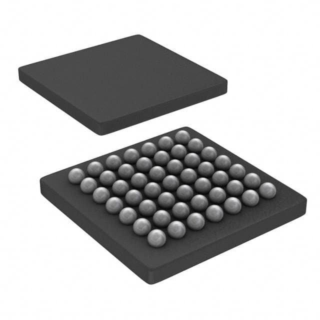
- Part No.:
- SN65LVDS311YFFT
- Manufacturer:
- Texas Instruments
- Category:
- Specialized
- Package:
- 49-UFBGA, DSBGA
- Datasheet:
-
 SN65LVDS311YFFT.pdf
- Description:
- IC INTFACE SPECIALIZED 49DSBGA
- Quantity:
- Payment:

- Shipping:

Inventory:153
Please send an inquiry. Send us your inquiry, and we will respond immediately.
Product details
Overview
SN65LVDS311 from Texas Instruments is a programmable 27-bit display serial interface transmitter that converts 24-bit RGB + 3 control + 1 parity + 2 reserved bits into SubLVDS serial streams over 1–3 differential links. It locks to pixel clocks from 4 MHz to 65 MHz, supports QVGA/VGA/XGA displays, and delivers sub-200 mV differential output swing with 0.9 V common-mode voltage.
For engineers reviewing the SN65LVDS311 datasheet, SN65LVDS311 pinout, SN65LVDS311 application, or SN65LVDS311 equivalent, this page provides verified technical context on serialization modes (1/2/3-channel), power management states (Active/Standby/Shutdown), SubLVDS electrical compliance, pixel clock jitter tolerance, and real-world timing latency across resolution-dependent configurations.
Technical Context
The SN65LVDS311 implements a PLL-based serializer with three configurable link modes: 1-channel (×30 PCLK multiplier, 4–15 MHz PCLK range), 2-channel (×15, 8–30 MHz), and 3-channel (×10, 20–65 MHz). Each mode determines active SubLVDS data pairs (D0 only; D0+D1; or D0+D1+D2) and internal clock division for CLK± recreation.
It features glitch-suppressed TXEN control (≥10 μs pulse width required), failsafe CMOS inputs, odd-parity generation over 27 payload bits, and automatic Standby entry when PCLK drops below 500 kHz. Power consumption scales with PCLK frequency and link count-e.g., 17.4 mW (QVGA, Active), 28.8 mW (VGA, Active), ≈0.5 μA (Shutdown).
Key Specifications
| Parameter | Value and Actual Design Meaning |
|---|---|
| Pixel Clock Range | 4–65 MHz, with mode-dependent bounds: 1ChM (4–15 MHz), 2ChM (8–30 MHz), 3ChM (20–65 MHz) |
| Differential Output Voltage (|VOD|) | 100–200 mV - meets SubLVDS standard for low-power, high-noise-immunity video interconnect |
| Common-Mode Output Voltage (VOCM) | 0.8–1.0 V - ensures compatibility with TI's SN65LVDS302 receiver and other SubLVDS receivers |
| Power Consumption (Active Mode) | 17.4 mW (QVGA), 28.8 mW (VGA), 44.5 mW (65 MHz) - enables thermal-aware layout in compact display modules |
| Propagation Delay (tpdL) | 0.8/fPCLK to 1.6/fPCLK seconds - deterministic latency critical for frame-synchronized camera-to-display pipelines |
| ESD Rating (HBM) | >3 kV - protects against handling damage during assembly of portable display subsystems |
| Input Signal Swing | 1.8 V CMOS - directly interfaces OMAP3630 and similar application processors without level-shifting |
Pinout & Package
SN65LVDS311YFFT uses a 2.8 × 2.8 mm, 40-pin QFN package (YFFT) with wettable flanks and exposed thermal pad. Pin assignment follows optimized routing for RGB parallel bus and SubLVDS differential pair fanout.
| Pin/Terminal | Circuit Role | Design Meaning |
|---|---|---|
| R0–R7, G0–G7, B0–B7 | CMOS RGB pixel data inputs | 24-bit parallel video bus; pin mapping depends on SWAP setting per datasheet Table 2 |
| PCLK | Input pixel clock | Latches parallel data on rising edge; PLL reference input; must be ≥500 kHz to avoid Standby |
| HS / VS / DE | Video timing control inputs | Horizontal sync, vertical sync, and data enable signals for embedded display interface compliance |
| LS0 / LS1 | Link select configuration | Set 1/2/3-channel serialization mode; floating not allowed - tie to VDD/GND per Table 3 |
| TXEN | Transmitter enable | Glitch-suppressed CMOS input; ≥10 μs high/low assertion required for reliable mode transitions |
| D0± / D1± / D2± | SubLVDS serial data outputs | Active per link mode; high-impedance when inactive - eliminates need for external termination switching |
| CLK± | SubLVDS pixel clock output | Recreated from internal PLL; fixed polarity; used by receiver for data recovery synchronization |
| VDD / VDDPLLA / VDDPLLD / VDDLVDS | Supply domains | Separate analog/digital/SubLVDS rails minimize noise coupling between PLL, logic, and I/O |
| GND / GNDPLLA / GNDPLLD / GNDLVDS | Ground domains | Isolated ground planes required per layout guidelines to maintain SubLVDS signal integrity |
Key Features
| Feature | Design Value |
|---|---|
| Programmable 1/2/3-channel serialization | Enables single PCB design to support QVGA through XGA resolutions via LS0/LS1 strap configuration |
| Integrated odd-parity generation | Protects 27-bit payload (24 RGB + HS/VS/DE) against single-bit errors - critical for medical and industrial displays |
| Automatic Standby on PCLK loss | Reduces current to <10 μA without external control - simplifies power sequencing in battery-powered cameras |
| SubLVDS-compliant outputs | 100–200 mV differential swing and 0.9 V common-mode meet TI SN65LVDS302 receiver requirements |
| Failsafe CMOS inputs | Prevents latch-up and leakage during power-up/power-down - eliminates need for external pull resistors on R/G/B/HS/VS/DE |
| Glitch-suppressed TXEN | Rejects transients <10 μs - avoids unintended shutdown during noisy system-level reset or hot-plug events |
Applications
| Embedded Camera Interface | Industrial LCD Display Module |
|---|---|
Use Scenario: High-resolution image sensor output routed to FPGA-based display controller over flexible cable. IC Role / Device Role / Timing Role: Serializer converting parallel MIPI D-PHY-like RGB bus into robust SubLVDS streams for EMI-sensitive environments. Use Value: 3-channel mode supports 65 MHz PCLK for 1080p@60fps with deterministic 1.1/fPCLK latency and built-in parity for error detection. |
Use Scenario: Compact HMI panel using OMAP3630 processor driving 800×480 TFT via 2-layer flex PCB. IC Role / Device Role / Timing Role: Bridge between processor's CMOS video port and display's SubLVDS receiver, managing HS/VS/DE timing alignment. Use Value: 2.8 × 2.8 mm YFFT package enables dense routing; 1.8 V input swing eliminates level shifters; 2ChM reduces EMI vs. single-link alternatives. |
| Medical Diagnostic Monitor | Automotive Infotainment Cluster |
Use Scenario: DICOM-compliant imaging display requiring zero-frame-loss transmission from GPU to panel. IC Role / Device Role / Timing Role: Fault-tolerant serializer with parity bit validation and failsafe inputs to prevent corrupted pixel data during boot or brownout. Use Value: Automatic Standby on PCLK stop prevents spurious output; >3 kV HBM ESD rating withstands clinical environment handling. |
Use Scenario: Dashboard cluster integrating instrument graphics and ADAS alerts onto shared LCD. IC Role / Device Role / Timing Role: Low-power display interface supporting dynamic resolution switching (QVGA for warning icons, VGA for maps). Use Value: Configurable link modes allow runtime power optimization: 1ChM for static UI (17.4 mW), 3ChM for full map rendering (44.5 mW). |
Equivalent & Alternatives
The following parts are listed as comparable options for similar display serializer applications.
| Alternative Part | Technical Difference | Application Difference | Selection Advice |
|---|---|---|---|
| SN65LVDS301 | 27-bit serializer with identical SubLVDS output specs but no parity bit generation or automatic Standby mode | Lacks error detection and PCLK-loss power management - requires external control logic for low-power states | Choose SN65LVDS311 when parity validation or autonomous power state transitions are required |
| SN65LVDS314 | Pin-compatible upgrade with extended PCLK range (up to 85 MHz), lower propagation delay (0.6/fPCLK), and improved jitter performance | Supports higher-resolution displays (e.g., WXGA) and tighter timing budgets in high-speed automotive clusters | Choose SN65LVDS314 for new designs targeting >65 MHz PCLK or stricter jitter budgets; SN65LVDS311 remains optimal for cost-sensitive QVGA/VGA systems |
Compared with SN65LVDS301, SN65LVDS311 adds parity and autonomous Standby-critical for reliability in unattended systems. Compared with SN65LVDS314, it trades higher max PCLK and lower latency for lower cost and proven qualification in legacy industrial displays.
Availability
SN65LVDS311 is available at Aetrix Electronics and suitable for embedded camera interfaces, industrial LCD display modules, medical diagnostic monitors, and automotive infotainment clusters requiring stable component supply across long production lifecycles.
Supply support for SN65LVDS311 includes scheduled delivery planning, volume procurement assistance, BOM continuity management, traceable sourcing, and lifecycle availability coordination for OEM customers, industrial embedded developers, connected-device designers, and electronics production programs.
Manufacturer
Texas Instruments is a global semiconductor leader specializing in analog, embedded processing, and connectivity technologies with decades of display interface IP expertise.
The SN65LVDS311 belongs to TI's LVDS display serializer family, designed specifically for low-power, high-reliability video transport between application processors and LCD panels in space-constrained, thermally sensitive systems.
FAQ
What is the maximum pixel clock frequency supported by the SN65LVDS311 in 3-channel mode?
The SN65LVDS311 supports up to 65 MHz pixel clock frequency in 3-channel mode, enabling high-resolution display formats such as VGA and XGA. This mode uses a ×10 PLL multiplication factor and requires PCLK ≥20 MHz to maintain lock. Operation above 65 MHz is not specified and may result in failed serialization or increased bit error rate.
Does the SN65LVDS311 generate its own pixel clock or only recreate the input PCLK?
The SN65LVDS311 does not generate an independent pixel clock; it recreates the input PCLK on the CLK± differential outputs using internal PLL-derived division. The recreated clock maintains phase coherence with the original PCLK and is essential for synchronous data recovery by compatible receivers like the SN65LVDS302.
How does the SN65LVDS311 handle power management when the pixel clock stops?
When the PCLK input stops or falls below 500 kHz, the SN65LVDS311 automatically enters Standby mode-shutting down the PLL and serializer while keeping the PCLK monitor active. Current drops to ≈0.5 μA, all outputs go high-impedance, and no external control is needed. This behavior is intrinsic to the SN65LVDS311 and requires no firmware intervention.
Can the SN65LVDS311 be used with non-TI SubLVDS receivers?
Yes-the SN65LVDS311 complies with standard SubLVDS electrical specifications: 100–200 mV differential output voltage, 0.8–1.0 V common-mode voltage, and 210 Ω differential output impedance. These parameters align with JEDEC and industry-standard SubLVDS receivers, though interoperability should be validated with specific receiver datasheets for timing margin and jitter tolerance.
What is the function of the two reserved bits added to the 30-bit serial frame?
The SN65LVDS311 adds two reserved bits (bit positions 28 and 29) to the 27-bit payload (24 RGB + HS/VS/DE) to form a fixed 30-bit serial frame. These bits are always transmitted as '0' and are not used for parity or control-they provide structural alignment for frame synchronization and future feature expansion without altering the core 27-bit data integrity model.
SN65LVDS311YFFT Specifications
- Product attributes
- Attribute value
- Manufacturer:
- Texas Instruments
- Series:
- 65LVDS
- Package/Case:
- 49-UFBGA, DSBGA
- Packaging:
- Tape & Reel (TR)
- Product Status:
- Active
- Applications:
- Cell Phone
- Interface:
- Serial
- Voltage - Supply:
- 1.65V ~ 1.95V
- Supplier Device Package:
- 49-DSBGA (2.8x2.8)
- Grade:
- -
- Qualification:
- -
- Mounting Type:
- Surface Mount
SN65LVDS311YFFT FAQ
1.How can I place an order for SN65LVDS311YFFT through Aetrix?
Please submit a Request for Quotation (RFQ) for SN65LVDS311YFFT on Aetrix. Our sales agent will provide a competitive quotation and guide you through the order confirmation once you accept the terms.
2.Are the price and stock information for SN65LVDS311YFFT reliable?
The price and inventory of SN65LVDS311YFFT are updated periodically and may fluctuate due to market conditions. Stock and pricing data are typically refreshed every 24 hours. Quotation validity for SN65LVDS311YFFT is usually 5 days.
3.What payment methods are accepted for SN65LVDS311YFFT?
We accept Wire Transfer, PayPal, Credit Card, Western Union, MoneyGram, and Escrow for SN65LVDS311YFFT transactions.
Note: Certain payment methods may incur a processing fee.
4.How is shipping managed for SN65LVDS311YFFT?
SN65LVDS311YFFT orders can be shipped via leading logistics carriers, including DHL, UPS, FedEx, TNT, or Registered Mail.
Once your SN65LVDS311YFFT order is processed, you will receive an email with the shipment details and tracking number.
Note: Tracking information may take up to 24 hours to appear. Express delivery typically takes 3–5 business days.
5.How can I obtain technical support or documentation for SN65LVDS311YFFT?
For technical support, including SN65LVDS311YFFT datasheets, pinout diagrams, or application guidance, please contact our engineering support team. They can provide detailed documentation and assistance for your SN65LVDS311YFFT requirements.
6.How does Aetrix verify that SN65LVDS311YFFT is sourced from the original manufacturer or authorized distributors?
All SN65LVDS311YFFT products on Aetrix are procured from qualified distributors and authorized channels. Our dedicated quality assurance team conducts strict verification, including traceability checks and, if necessary, third-party testing. This ensures that SN65LVDS311YFFT meets industry standards.
7.What is the process for return or replacement of SN65LVDS311YFFT?
All SN65LVDS311YFFT units undergo pre-shipment inspection (PSI). If there is an issue with SN65LVDS311YFFT, returns or replacements are accepted under the following conditions:
1.Quantity discrepancies, incorrect items, or visible external defects (such as breakage or corrosion), acknowledged by Aetrix.
2.The issue is reported within 90 days of delivery.
3.The SN65LVDS311YFFT part is unused and in its original packaging.
Return procedure for SN65LVDS311YFFT:
1.Submit a request within 90 days.
2.Obtain a Return Material Authorization (RMA) from Aetrix.
SN65LVDS311YFFT Tags

-
NVT4857UKAZ
NXP Semiconductors

-
TCA8418RTWR
Texas Instruments

-
PCA9546APWR
Texas Instruments

-
MD0100N8-G
Microchip Technology

-
PCA9548APW,118
NXP Semiconductors

-
PCA9540BDP,118
NXP Semiconductors

-
PCA9548APWR
Texas Instruments

-
PCA9546APW,118
NXP Semiconductors

-
PTN3360DBS,518
NXP Semiconductors

-
PCA9546ABS,118
NXP Semiconductors

-
PCA9518PWR
Texas Instruments

-
PCA9545APW,118
NXP Semiconductors
Tech Hub

A practical engineering guide to 3.3V and 5V logic compatibility, input thresholds, resistor dividers, translator ICs, MOSFET level shifting, I2C pull-ups, timing limits and power-sequencing risks.

The 74HC595 uses push-pull logic outputs, while the TPIC6B595 uses 50 V open-drain DMOS sinks for higher-power loads. This guide compares timing, current limits, 3.3 V interfacing, load wiring, thermal…

The 74HC595 converts serial data into eight stable parallel outputs. This guide covers pin functions, shift and storage timing, OE and MR behavior, drive-current limits, cascading, voltage compatibilit…

A technical comparison of level-sensitive latches and edge-triggered flip-flops, covering timing windows, setup and hold limits, master–slave operation, time borrowing, race-through, HDL inference and…

A D latch stores one bit while Enable controls when data can pass. This reference covers gate-level operation, truth tables, transparency, setup and hold timing, LE versus OE, common ICs and practical …

An SR latch stores one bit through cross-coupled feedback. This engineering reference covers NOR and NAND implementations, truth tables, forbidden-state recovery, gated operation, switch debouncing, fa…

Latch circuits retain one bit through feedback. This technical reference covers SR and D latches, truth tables, transparency, timing limits, latch-versus-flip-flop behavior, applications and common log…

An engineering guide to LED driver operation, constant-current and constant-voltage outputs, linear and switching topologies, dimming, IC selection, calculations, replacement compatibility, and fault c…

Operational amplifier guide covering op amp basics, feedback, ideal vs real op amps, common configurations, buffer circuits, offset, bias current, gain-bandwidth, slew rate, rail-to-rail limits and sel…

Jumper cables guide covering safe connection order, red and black clamp placement, final ground connection, cable gauge, length, clamp quality, copper vs CCA cables, jump starter comparison and battery…


