
 My Inquiry
 My Account


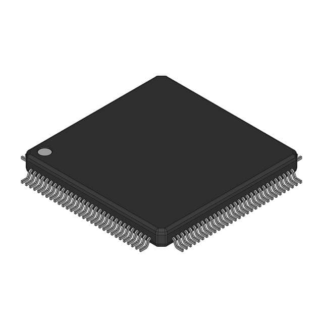
Texas Instruments SN74ABT3612-30PCB
- Part No.:
- SN74ABT3612-30PCB
- Manufacturer:
- Texas Instruments
- Category:
- FIFOs Memory
- Package:
- 120-LQFP
- Datasheet:
-
 SN74ABT3612-30PCB.pdf
- Description:
- IC FIFO SYNC 64X36X2 120HLQFP
- Quantity:
- Payment:

- Shipping:

Inventory:3,100
Please send an inquiry. Send us your inquiry, and we will respond immediately.
Product details
Overview
SN74ABT3612-30PCB from Texas Instruments is a clocked bidirectional FIFO memory IC with two independent 64 × 36 dual-port SRAM buffers, supporting asynchronous or coincident CLKA/CLKB operation up to 67 MHz, 10 ns read access time, and passive parity checking on both 36-bit ports. It enables high-throughput data buffering between mismatched microprocessor buses in telecom backplanes.
For engineers reviewing the SN74ABT3612-30PCB datasheet, SN74ABT3612-30PCB pinout, SN74ABT3612-30PCB application, or SN74ABT3612-30PCB equivalent, key selection criteria include dual-clock domain synchronization, programmable almost-full/empty flag offsets (4–16 words), mailbox-bypass register support, and BiCMOS low-power timing performance at industrial temperature range (0°C to 70°C).
Technical Context
The SN74ABT3612-30PCB implements two independent clocked FIFOs (FIFO1 and FIFO2), each with separate write/read pointers, full/empty flag logic, and two-stage synchronizers for all status flags-EFA/FFA/AEA/AFA synchronized to CLKA, EFB/FFB/AEB/AFB to CLKB. Its mailbox registers (mail1/mail2) provide zero-latency command handshaking without queuing delay.
Flag offset programming uses FS0/FS1 latched on RST rising edge to select 4, 8, 12, or 16-word thresholds for almost-full and almost-empty conditions. Parity generation (PGA/PGB) and checking (PEFA/PEFB) operate per-byte (4 × 9-bit groups) with ODD/EVEN-selectable mode, sharing parity trees between port inputs and mailbox outputs.
Key Specifications
| Parameter | Value and Actual Design Meaning |
|---|---|
| Memory Depth × Width × Ports | 64 × 36 × 2 independent FIFOs-enables simultaneous bidirectional buffering of 36-bit data streams with 64-word depth per direction. |
| Max Clock Frequency | 67 MHz-supports high-speed interconnect between PCI, VME, or custom parallel buses without throttling throughput. |
| Read Access Time | 10 ns-guarantees sub-15 ns latency for FIFO output register reads under worst-case industrial conditions. |
| Operating Temperature | 0°C to 70°C-validated for commercial/industrial embedded systems where ambient thermal cycling occurs. |
| Supply Voltage | 5 V ± 5%-compatible with legacy TTL/ABT logic families and eliminates need for level-shifting in 5-V systems. |
| Parity Support | Per-port byte-level parity check/generation (4 × 9-bit groups)-detects single-bit errors on A0–A35 and B0–B35 with selectable odd/even mode. |
| Flag Synchronization | Two-stage flip-flop sync per flag-reduces metastability risk when CLKA and CLKB operate asynchronously across clock domains. |
Pinout & Package
SN74ABT3612-30PCB is housed in a 120-pin Thin Quad Flat Package (TQFP), designated PCB in TI documentation, with 0.4 mm lead pitch and exposed thermal pad. Pin numbering follows standard top-view orientation with corner pin #1 marked.
| Pin/Terminal | Circuit Role | Design Meaning |
|---|---|---|
| A0–A35, B0–B35 | 36-bit bidirectional data ports | Independent I/O lanes for Port-A and Port-B; high-impedance when CSA/CSB or W/RA/W/RB high-enables bus sharing without external transceivers. |
| CLKA, CLKB | Asynchronous port clocks | Continuous free-running clocks; all transfers gated on low-to-high transition-allows independent clock domain operation or synchronous alignment. |
| ENA, ENB | Port enable controls | High-active enables for CLKA/CLKB sampling-prevents spurious writes/reads during clock startup or glitch periods. |
| CSA, CSB | Chip select inputs | Active-low enables for port access-permits multiple SN74ABT3612-30PCB devices on shared data buses using address decoding. |
| EFA/EFB, FFA/FFB | Synchronized empty/full flags | Two-stage synced outputs indicate FIFO state relative to CLKA/CLKB-ensures reliable handshake signaling across clock boundaries. |
| AEA/AEB, AFA/AFB | Programmable almost-empty/full flags | Configurable threshold flags (4/8/12/16 words) latched on RST↑-enables early flow control before buffer exhaustion or overflow. |
| MBA, MBB | Mailbox select inputs | Selects mail1/mail2 register instead of FIFO output-provides deterministic latency bypass path for control messages or DMA setup. |
| RST | Asynchronous reset input | Four CLKA + four CLKB transitions required for full initialization-ensures pointer and flag consistency across both clock domains. |
Key Features
| Feature | Design Value |
|---|---|
| Dual independent clock domains | CLKA and CLKB support fully asynchronous operation or precise coincidence-eliminates need for clock domain crossing logic in heterogeneous systems. |
| Mailbox-bypass registers | Two 36-bit mail1/mail2 registers with MBF1/MBF2 handshaking flags-enables immediate command transfer without FIFO queuing delay or pointer management. |
| Programmable flag offsets | FS0/FS1 select 4, 8, 12, or 16-word thresholds for AFA/AEA/AFB/AEB-allows fine-grained flow control tuning for varying burst lengths and latency budgets. |
| Shared parity hardware | Same parity trees serve port inputs and mailbox outputs-reduces die area while maintaining error detection integrity for both buffered and bypassed data paths. |
| BiCMOS process technology | Combines bipolar speed with CMOS power efficiency-delivers 67 MHz operation at <200 mW typical active power, suitable for dense backplane modules. |
Applications
| Telecom Line Card Buffering | Industrial PLC Data Aggregation |
|---|---|
Use Scenario: Buffering packetized voice/data between TDM framer and ATM switch fabric operating at different clock rates. IC Role / Device Role / Timing Role: Clocked FIFO bridging asynchronous 8 kHz TDM and 622 Mbps ATM clock domains with deterministic latency and lossless framing. Use Value: Eliminates bit slips and frame misalignment by absorbing clock drift via dual 64-word depth, while mailbox registers pass control signals (e.g., alarm triggers) with zero FIFO delay. | Use Scenario: Consolidating sensor readings from multiple RS-485 fieldbus nodes into a central controller with variable scan intervals. IC Role / Device Role / Timing Role: Bidirectional FIFO managing bursty analog input acquisition and deterministic output actuation commands across non-synchronous scan cycles. Use Value: Prevents data overrun during peak sensor sampling and ensures timely actuator updates using programmable almost-full/empty flags to throttle upstream acquisition rate. |
| PCI-to-Local Bus Bridge | Medical Imaging Data Pipeline |
Use Scenario: Interfacing 33 MHz PCI bus to custom 50 MHz imaging processor local bus with differing burst protocols. IC Role / Device Role / Timing Role: Dual-port FIFO decoupling PCI master writes and local bus reads, with mailbox registers delivering DMA descriptors ahead of payload transfers. Use Value: Achieves sustained 264 MB/s throughput (33 MHz × 8 bytes) while isolating PCI arbitration delays from real-time image processing deadlines. | Use Scenario: Streaming raw pixel data from CT detector array to reconstruction engine with strict jitter tolerance (<5 ns cycle-to-cycle variation). IC Role / Device Role / Timing Role: Low-jitter FIFO providing 10 ns access time and two-stage flag synchronization to meet DICOM latency constraints. Use Value: Guarantees sub-microsecond end-to-end latency for 16-bit pixel words, with parity checking ensuring data integrity across radiation-prone environments. |
Equivalent & Alternatives
The following parts are listed as comparable options for similar clocked FIFO applications.
| Alternative Part | Technical Difference | Application Difference | Selection Advice |
|---|---|---|---|
| IDT72V2105L15PF | 3.3 V supply, 15 ns access, 256 × 18 depth, LVDS-compatible I/O | Better suited for modern low-voltage, high-density designs; lacks mailbox registers and programmable flag offsets | Choose IDT72V2105L15PF when migrating to 3.3 V systems and requiring higher density over 36-bit width. |
| SN74ACT2227DW | 5 V supply, 2 × 256 × 9 FIFOs, no mailbox, no parity, 12 ns access | Higher depth but narrower width; simpler control interface without flag offset programming | Choose SN74ACT2227DW for cost-sensitive 5 V applications needing deeper buffering without advanced flow control features. |
Compared with IDT72V2105L15PF and SN74ACT2227DW, SN74ABT3612-30PCB uniquely delivers 36-bit width, mailbox bypass, and programmable flag thresholds in a 5 V BiCMOS package-making it optimal for legacy telecom and industrial backplanes requiring deterministic latency and robust error handling.
Availability
SN74ABT3612-30PCB is available at Aetrix Electronics and suitable for telecom line card design, industrial PLC data aggregation, PCI-to-local bus bridging, and medical imaging data pipeline applications requiring stable component supply and long-term obsolescence management.
Supply support for SN74ABT3612-30PCB includes scheduled delivery planning, volume procurement assistance, BOM continuity management, traceable sourcing, and lifecycle availability coordination for OEM customers, industrial embedded developers, connected-device designers, and electronics production programs.
Manufacturer
Texas Instruments is a global semiconductor leader specializing in analog, embedded processing, and logic solutions, with decades of heritage in high-reliability interface and memory products.
The SN74ABT3612-30PCB belongs to TI's ABT logic family-designed specifically for high-speed, low-power bidirectional data buffering in multi-clock-domain systems such as telecom infrastructure and industrial automation controllers.
FAQ
What is the maximum supported clock frequency for SN74ABT3612-30PCB?
The SN74ABT3612-30PCB supports clock frequencies up to 67 MHz on both CLKA and CLKB inputs under industrial temperature conditions (0°C to 70°C). This rating is validated per the SCBS129G datasheet and reflects guaranteed timing margins for setup/hold and propagation delays in the BiCMOS process.
Does SN74ABT3612-30PCB support independent clock domains?
Yes, SN74ABT3612-30PCB explicitly supports asynchronous operation of CLKA and CLKB-its flags (EFA/FFA/AEA/AFA and EFB/FFB/AEB/AFB) are independently synchronized to their respective clocks using two-stage flip-flop chains, enabling reliable handshaking across unrelated clock domains.
How are the almost-full and almost-empty flag thresholds programmed on SN74ABT3612-30PCB?
The SN74ABT3612-30PCB uses FS0 and FS1 inputs, latched on the rising edge of RST, to select one of four preset offset values (4, 8, 12, or 16 words) for both AFA/AEA and AFB/AEB flags. This allows precise tuning of early flow control without firmware intervention.
What is the function of the mailbox registers in SN74ABT3612-30PCB?
SN74ABT3612-30PCB includes two 36-bit mailbox registers (mail1 and mail2) that allow immediate data transfer between Port-A and Port-B without FIFO queuing delay. MBA and MBB select mailbox access, while MBF1 and MBF2 provide hardware handshaking to prevent overwrite and ensure atomic delivery.
Can SN74ABT3612-30PCB perform parity generation and checking simultaneously on both ports?
Yes, SN74ABT3612-30PCB supports concurrent parity generation (via PGA/PGB) and checking (via PEFA/PEFB) on both ports. Parity is computed per 9-bit byte (A0–A8, etc.), with ODD/EVEN selecting mode, and the same parity trees serve both port inputs and mailbox outputs-ensuring consistent error detection across all data paths.
SN74ABT3612-30PCB Specifications
- Product attributes
- Attribute value
- Manufacturer:
- Texas Instruments
- Series:
- 74ABT
- Package/Case:
- 120-LQFP
- Packaging:
- Tray
- Product Status:
- Obsolete
- Programmable:
- Not Verified
- Memory Size:
- 4.5K (64 x 36 x 2)
- Function:
- Synchronous
- Data Rate:
- 33.4MHz
- Access Time:
- 15ns
- Voltage - Supply:
- 4.5 V ~ 5.5 V
- Current - Supply (Max):
- 130mA
- Bus Directional:
- Bi-Directional
- Expansion Type:
- Width
- Programmable Flags Support:
- Yes
- Retransmit Capability:
- No
- FWFT Support:
- No
- Operating Temperature:
- 0°C ~ 70°C
- Mounting Type:
- Surface Mount
- Supplier Device Package:
- 120-HLQFP (14x14)
SN74ABT3612-30PCB FAQ
1.How can I place an order for SN74ABT3612-30PCB through Aetrix?
Please submit a Request for Quotation (RFQ) for SN74ABT3612-30PCB on Aetrix. Our sales agent will provide a competitive quotation and guide you through the order confirmation once you accept the terms.
2.Are the price and stock information for SN74ABT3612-30PCB reliable?
The price and inventory of SN74ABT3612-30PCB are updated periodically and may fluctuate due to market conditions. Stock and pricing data are typically refreshed every 24 hours. Quotation validity for SN74ABT3612-30PCB is usually 5 days.
3.What payment methods are accepted for SN74ABT3612-30PCB?
We accept Wire Transfer, PayPal, Credit Card, Western Union, MoneyGram, and Escrow for SN74ABT3612-30PCB transactions.
Note: Certain payment methods may incur a processing fee.
4.How is shipping managed for SN74ABT3612-30PCB?
SN74ABT3612-30PCB orders can be shipped via leading logistics carriers, including DHL, UPS, FedEx, TNT, or Registered Mail.
Once your SN74ABT3612-30PCB order is processed, you will receive an email with the shipment details and tracking number.
Note: Tracking information may take up to 24 hours to appear. Express delivery typically takes 3–5 business days.
5.How can I obtain technical support or documentation for SN74ABT3612-30PCB?
For technical support, including SN74ABT3612-30PCB datasheets, pinout diagrams, or application guidance, please contact our engineering support team. They can provide detailed documentation and assistance for your SN74ABT3612-30PCB requirements.
6.How does Aetrix verify that SN74ABT3612-30PCB is sourced from the original manufacturer or authorized distributors?
All SN74ABT3612-30PCB products on Aetrix are procured from qualified distributors and authorized channels. Our dedicated quality assurance team conducts strict verification, including traceability checks and, if necessary, third-party testing. This ensures that SN74ABT3612-30PCB meets industry standards.
7.What is the process for return or replacement of SN74ABT3612-30PCB?
All SN74ABT3612-30PCB units undergo pre-shipment inspection (PSI). If there is an issue with SN74ABT3612-30PCB, returns or replacements are accepted under the following conditions:
1.Quantity discrepancies, incorrect items, or visible external defects (such as breakage or corrosion), acknowledged by Aetrix.
2.The issue is reported within 90 days of delivery.
3.The SN74ABT3612-30PCB part is unused and in its original packaging.
Return procedure for SN74ABT3612-30PCB:
1.Submit a request within 90 days.
2.Obtain a Return Material Authorization (RMA) from Aetrix.
SN74ABT3612-30PCB Tags
-
7201LA15JGI
Renesas
-
7204L12JG
Renesas

-
72V82L15PAG8
Renesas

-
7205L15JGI
Renesas
-
7208L20JG
Renesas

-
72V2105L10PFG
Renesas
-
72V2111L15PFGI
Renesas

-
72V2113L6PFG
Renesas
-
72V36110L6PFG
Renesas

-
SN74ALVC7804-40DL
Texas Instruments
-
7202LA25JGI
Renesas
-
SN74V245-15PAG
Texas Instruments
Tech Hub

A practical engineering guide to 3.3V and 5V logic compatibility, input thresholds, resistor dividers, translator ICs, MOSFET level shifting, I2C pull-ups, timing limits and power-sequencing risks.

The 74HC595 uses push-pull logic outputs, while the TPIC6B595 uses 50 V open-drain DMOS sinks for higher-power loads. This guide compares timing, current limits, 3.3 V interfacing, load wiring, thermal…

The 74HC595 converts serial data into eight stable parallel outputs. This guide covers pin functions, shift and storage timing, OE and MR behavior, drive-current limits, cascading, voltage compatibilit…

A technical comparison of level-sensitive latches and edge-triggered flip-flops, covering timing windows, setup and hold limits, master–slave operation, time borrowing, race-through, HDL inference and…

A D latch stores one bit while Enable controls when data can pass. This reference covers gate-level operation, truth tables, transparency, setup and hold timing, LE versus OE, common ICs and practical …

An SR latch stores one bit through cross-coupled feedback. This engineering reference covers NOR and NAND implementations, truth tables, forbidden-state recovery, gated operation, switch debouncing, fa…

Latch circuits retain one bit through feedback. This technical reference covers SR and D latches, truth tables, transparency, timing limits, latch-versus-flip-flop behavior, applications and common log…

An engineering guide to LED driver operation, constant-current and constant-voltage outputs, linear and switching topologies, dimming, IC selection, calculations, replacement compatibility, and fault c…

Operational amplifier guide covering op amp basics, feedback, ideal vs real op amps, common configurations, buffer circuits, offset, bias current, gain-bandwidth, slew rate, rail-to-rail limits and sel…

Jumper cables guide covering safe connection order, red and black clamp placement, final ground connection, cable gauge, length, clamp quality, copper vs CCA cables, jump starter comparison and battery…


