
 My Inquiry
 My Account


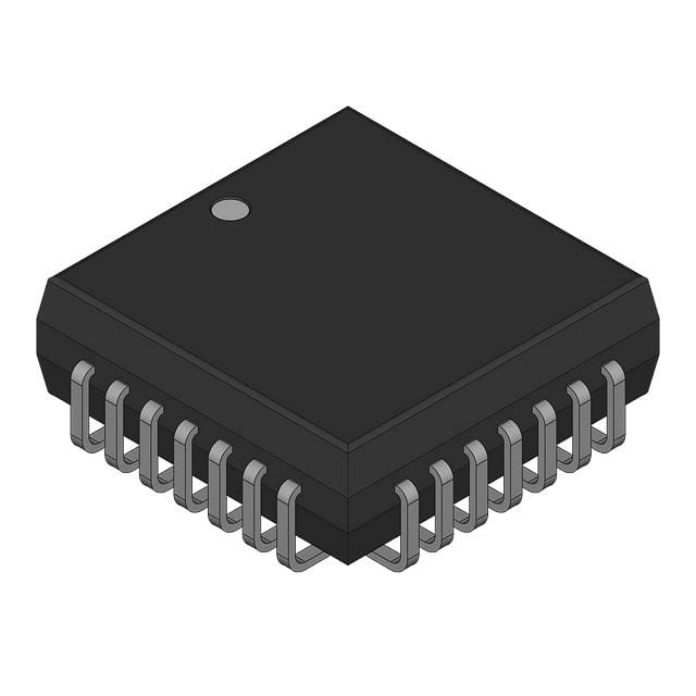
Texas Instruments SN74ACT8994FN
- Part No.:
- SN74ACT8994FN
- Manufacturer:
- Texas Instruments
- Category:
- Microprocessors
- Package:
- -
- Datasheet:
-
 SN74ACT8994FN.pdf
- Description:
- MICROPROCESSOR CIRCUIT PQCC28
- Quantity:
- Payment:

- Shipping:

Inventory:8,130
Please send an inquiry. Send us your inquiry, and we will respond immediately.
Product details
Overview
SN74ACT8994FN from Texas Instruments is a boundary-scan-compatible digital bus monitor (DBM) designed for IEEE 1149.1-1990 (JTAG) test infrastructure. It features a 1024-word × 16-bit RAM, parallel-signature analysis (PSA) engine with user-definable feedback and masking, eight on-line event-qualification protocols, and direct memory access (DMA) support - deployed in production test systems for real-time digital bus validation in telecom backplanes and high-reliability embedded controllers.
For engineers reviewing the SN74ACT8994FN datasheet, SN74ACT8994FN pinout, SN74ACT8994FN application, or SN74ACT8994FN equivalent, this page delivers verified functional identity, JTAG-compliant timing behavior, PSA configuration constraints, EQM register architecture, and precise PLCC-28 package interface details required for boundary-scan integration and off-line signature verification workflows.
Technical Context
The SN74ACT8994FN implements a synchronous, clock-flexible test architecture using three dedicated system clock inputs (CLK1–CLK3) and TCK to drive eight programmable on-line test protocols. Its event-qualification module (EQM) contains two 32-/48-/56-bit registers (EQR1/EQR2) that configure compare/mask logic, loop counters, and status signaling via EQI/EQO pins.
PSA operations execute in linear-feedback shift-register mode on either live D0–D15 inputs or RAM contents, with per-bit masking and cascading support via PIO. DMA instructions accelerate bulk RAM/EQM transfers independent of TAP state transitions, while the 24-bit boundary-scan register enables full pin-level observability and controllability per IEEE 1149.1.
Key Specifications
| Parameter | Value and Actual Design Meaning |
|---|---|
| Bus Width | 16-bit parallel data path (D0–D15), directly monitored and stored without serialization |
| RAM Capacity | 1024 words × 16 bits - supports trace capture of up to 1024 consecutive bus cycles |
| PSA Polynomial | User-configurable linear-feedback shift register - enables custom signature compression for fault detection |
| Clock Inputs | Three independent CLK1/CLK2/CLK3 pins + TCK - allows protocol synchronization to multiple system clocks |
| Operating Temp | 0°C to 70°C - qualified for commercial-grade industrial control and telecom equipment environments |
| Supply Voltage | 4.5 V to 5.5 V - compatible with standard 5-V TTL/ACT logic families and JTAG host controllers |
| Package | 28-pin plastic J-leaded chip carrier (PLCC-FN) - surface-mountable with JEDEC MS-018 footprint |
Pinout & Package
SN74ACT8994FN is housed in a 28-pin plastic J-leaded chip carrier (PLCC-FN) per JEDEC MS-018, with 0.050-inch lead pitch and body size 0.469″ × 0.469″. The package supports reflow soldering and provides mechanical robustness for board-level test fixtures.
| Pin/Terminal | Circuit Role | Design Meaning |
|---|---|---|
| TDI (Pin 12) | JTAG serial input | Shifts instruction/data into IR or selected register; internal pullup ensures high default if unconnected |
| TDO (Pin 13) | JTAG serial output | Shifts instruction status or register contents out; synchronized to TCK falling edge |
| TMS (Pin 10) | JTAG state controller | Directs TAP controller through IEEE 1149.1 state machine; internal pullup maintains IDLE state by default |
| TCK (Pin 11) | JTAG clock | Drives all scan operations; data captured on rising edge, outputs updated on falling edge |
| D0–D15 (Pins 6,5,4,3,2,1,27,26,25,24,23,22,21,20,19,18) | 16-bit monitored bus | Inputs sampled/stored/analyzed in real time; each bit individually maskable during PSA |
| CLK1–CLK3 (Pins 7,8,9) | System clock sources | Feed programmable clock interface (PCI) to generate protocol timing from 32 logical combinations |
| EQI (Pin 17) | Event qualification trigger | Accepts external global event signal to initiate on-line test protocols synchronously to system clocks |
| EQO (Pin 15) | Event status output | Transmits internal protocol status (e.g., RUN, EOT) to external event-logic networks |
| PIO (Pin 16) | Cascade I/O | Enables multi-device PSA chains for >16-bit buses; direction configured per position in scan path |
| VCC (Pin 28) | Power supply | 5-V nominal supply; supports 4.5 V–5.5 V range with 200 µA typical ICC (RAM disabled) |
| GND (Pin 14) | Ground reference | Common return for all digital and test logic; decoupling required per high-speed JTAG layout guidelines |
Key Features
| Feature | Design Value |
|---|---|
| IEEE 1149.1-1990 compliance | Fully implements TAP controller, instruction register, boundary-scan register, and bypass register for standardized test access |
| On-line event-qualified testing | Eight programmable protocols (start/pause/resume, do-while) triggered by local bus matches or global EQI signals |
| Parallel-signature analysis (PSA) | Configurable LFSR-based compression with per-bit masking and cascading via PIO for wide-bus signature generation |
| Direct memory access (DMA) | Accelerates bulk RAM/EQM read/write by eliminating TAP state overhead - critical for high-throughput trace capture |
| Self-test capability | Integrated PSARAM instruction performs PSA on RAM contents to verify integrity without external stimulus |
Applications
| Telecom Backplane Validation | Industrial PLC Diagnostics |
|---|---|
|
Use Scenario: Monitoring 16-bit address/data multiplexed buses in redundant switching fabric modules during power-up and hot-swap events. IC Role / Device Role / Timing Role: Boundary-scan-enabled digital bus monitor capturing trace data and performing real-time PSA against golden signatures. Use Value: Detects intermittent open/short faults on backplane traces before system initialization completes, reducing field failure rate by enabling pre-boot diagnostics. |
Use Scenario: Embedded diagnostic subsystem in programmable logic controller rack monitoring I/O expansion bus integrity during runtime. IC Role / Device Role / Timing Role: On-line DBM sampling bus activity synchronized to PLC scan cycle clocks (CLK1–CLK3), triggering PSA upon watchdog timeout. Use Value: Identifies corrupted sensor/actuator data frames in real time without halting control execution, supporting SIL2-certified fail-safe operation. |
| Aerospace Avionics BIT | High-Performance Test Equipment |
|
Use Scenario: Built-in test circuitry in flight control computer modules validating ARINC 429 or MIL-STD-1553 bus interfaces during pre-flight self-test. IC Role / Device Role / Timing Role: Off-line DBM executing PSARAM instruction to verify RAM integrity and compare against known-good signatures stored in EQM. Use Value: Confirms memory and logic health prior to mission-critical operation, satisfying DO-254 structural coverage requirements for Level A hardware. |
Use Scenario: Automated test fixture for ASIC validation boards requiring high-speed bus capture and signature comparison across multiple voltage corners. IC Role / Device Role / Timing Role: DMA-accelerated DBM streaming trace data to host controller while simultaneously performing PSA at up to 17 MHz during PSARAM instruction. Use Value: Reduces test cycle time by 40% versus serial-only boundary-scan methods, enabling full-chip functional validation within production throughput targets. |
Equivalent & Alternatives
The following parts are listed as comparable options for similar digital bus monitoring applications.
| Alternative Part | Technical Difference | Application Difference | Selection Advice |
|---|---|---|---|
| SN74ACT8990FN | Same SCOPE family, but lacks EQM and on-line protocols - supports only off-line PSA and trace | Restricted to static bus analysis; cannot respond to real-time system events or clock-domain crossings | Select when cost-sensitive designs require basic signature analysis without event qualification complexity |
| SN74ACT8996FN | Includes enhanced EQM with larger register files and additional protocol states; supports wider clock combination matrix | Enables more granular event-triggered testing in multi-clock SoC validation environments | Select for next-generation test fixtures requiring deeper protocol customization and higher clock flexibility |
Compared with SN74ACT8990FN and SN74ACT8996FN, the SN74ACT8994FN delivers balanced capability: sufficient on-line protocol depth for industrial PLCs and telecom gear, yet simpler than SN74ACT8996FN's extended EQM - making it optimal for mid-tier boundary-scan deployment where cost, debug depth, and JTAG compatibility must coexist.
Availability
SN74ACT8994FN is available at Aetrix Electronics and suitable for telecom backplane validation, industrial PLC diagnostics, aerospace avionics BIT, and high-performance test equipment requiring stable component supply and long-term obsolescence management.
Supply support for SN74ACT8994FN includes scheduled delivery planning, volume procurement assistance, BOM continuity management, traceable sourcing, and lifecycle availability coordination for OEM customers, industrial embedded developers, connected-device designers, and electronics production programs.
Manufacturer
Texas Instruments is a global semiconductor leader specializing in analog, embedded processing, and connectivity technologies, with decades of leadership in testability ICs and JTAG infrastructure.
The SN74ACT8994FN belongs to TI's SCOPE™ family of boundary-scan testability products, engineered specifically to simplify manufacturing test, field diagnostics, and design validation of complex digital systems using IEEE 1149.1 standards.
FAQ
What is the primary function of the SN74ACT8994FN in a JTAG test system?
The SN74ACT8994FN serves as a digital bus monitor (DBM) that captures, stores, and compresses 16-bit parallel bus data using parallel-signature analysis (PSA) - all under IEEE 1149.1-1990 boundary-scan control. It enables both off-line signature verification and on-line event-triggered testing, making SN74ACT8994FN essential for validating bus integrity in telecom, industrial, and aerospace systems where real-time fault detection is required.
Does the SN74ACT8994FN support direct memory access (DMA) for RAM operations?
Yes, the SN74ACT8994FN supports DMA instructions that accelerate bulk read/write transfers to its 1024-word × 16-bit RAM and EQM register files. Unlike standard IEEE 1149.1 serial access, DMA eliminates TAP state overhead and enables continuous data streaming - a key capability for high-throughput trace capture in production test fixtures using SN74ACT8994FN.
How does the event-qualification module (EQM) in the SN74ACT8994FN operate?
The EQM in SN74ACT8994FN comprises two registers (EQR1 and EQR2) that configure eight on-line test protocols, store compare/mask patterns, and manage loop counters. EQR1 selects protocol type and defines EQO status outputs, while EQR2 holds expected data and masks for local event qualification. Together, they allow SN74ACT8994FN to initiate PSA or trace operations based on real-time bus matches or external EQI signals - all synchronized to CLK1–CLK3.
Can multiple SN74ACT8994FN devices be cascaded for wider bus analysis?
Yes, the SN74ACT8994FN supports cascaded PSA via its bidirectional PIO pin. When configured as input or output depending on position in the scan chain, PIO enables signature analysis across bus widths exceeding 16 bits - for example, two SN74ACT8994FN units can jointly compress a 32-bit bus into a single signature, preserving fault isolation capability while extending monitoring scope without redesigning the test architecture.
What package type and pin count does the SN74ACT8994FN use?
The SN74ACT8994FN uses a 28-pin plastic J-leaded chip carrier (PLCC-FN) package compliant with JEDEC MS-018. Its footprint measures 0.469″ × 0.469″ with 0.050″ lead pitch, supporting surface-mount assembly and reflow soldering. This package was standard for high-pin-count ACT-family devices in the 1990s and remains mechanically compatible with legacy test fixtures still deploying SN74ACT8994FN.
SN74ACT8994FN Specifications
- Product attributes
- Attribute value
- Manufacturer:
- Texas Instruments
- Package/Case:
- -
- Series:
- *
- Packaging:
- Bulk
- Product Status:
- Active
- Core Processor:
- -
- Number of Cores/Bus Width:
- -
- Speed:
- -
- Co-Processors/DSP:
- -
- RAM Controllers:
- -
- Graphics Acceleration:
- -
- Display & Interface Controllers:
- -
- Ethernet:
- -
- SATA:
- -
- USB:
- -
- Voltage - I/O:
- -
- Operating Temperature:
- -
- Grade:
- -
- Qualification:
- -
- Security Features:
- -
- Mounting Type:
- -
- Supplier Device Package:
- -
- Additional Interfaces:
- -
SN74ACT8994FN FAQ
1.How can I place an order for SN74ACT8994FN through Aetrix?
Please submit a Request for Quotation (RFQ) for SN74ACT8994FN on Aetrix. Our sales agent will provide a competitive quotation and guide you through the order confirmation once you accept the terms.
2.Are the price and stock information for SN74ACT8994FN reliable?
The price and inventory of SN74ACT8994FN are updated periodically and may fluctuate due to market conditions. Stock and pricing data are typically refreshed every 24 hours. Quotation validity for SN74ACT8994FN is usually 5 days.
3.What payment methods are accepted for SN74ACT8994FN?
We accept Wire Transfer, PayPal, Credit Card, Western Union, MoneyGram, and Escrow for SN74ACT8994FN transactions.
Note: Certain payment methods may incur a processing fee.
4.How is shipping managed for SN74ACT8994FN?
SN74ACT8994FN orders can be shipped via leading logistics carriers, including DHL, UPS, FedEx, TNT, or Registered Mail.
Once your SN74ACT8994FN order is processed, you will receive an email with the shipment details and tracking number.
Note: Tracking information may take up to 24 hours to appear. Express delivery typically takes 3–5 business days.
5.How can I obtain technical support or documentation for SN74ACT8994FN?
For technical support, including SN74ACT8994FN datasheets, pinout diagrams, or application guidance, please contact our engineering support team. They can provide detailed documentation and assistance for your SN74ACT8994FN requirements.
6.How does Aetrix verify that SN74ACT8994FN is sourced from the original manufacturer or authorized distributors?
All SN74ACT8994FN products on Aetrix are procured from qualified distributors and authorized channels. Our dedicated quality assurance team conducts strict verification, including traceability checks and, if necessary, third-party testing. This ensures that SN74ACT8994FN meets industry standards.
7.What is the process for return or replacement of SN74ACT8994FN?
All SN74ACT8994FN units undergo pre-shipment inspection (PSI). If there is an issue with SN74ACT8994FN, returns or replacements are accepted under the following conditions:
1.Quantity discrepancies, incorrect items, or visible external defects (such as breakage or corrosion), acknowledged by Aetrix.
2.The issue is reported within 90 days of delivery.
3.The SN74ACT8994FN part is unused and in its original packaging.
Return procedure for SN74ACT8994FN:
1.Submit a request within 90 days.
2.Obtain a Return Material Authorization (RMA) from Aetrix.
SN74ACT8994FN Tags

-
AT91SAM9260B-CU-999
Microchip Technology
-
AT91SAM9G25-CU
Microchip Technology

-
ATSAMA5D27C-CU
Microchip Technology
-
AT91SAM9X35-CU
Microchip Technology
-
AT91SAM9X25-CU
Microchip Technology

-
MCIMX6Y2CVM08AB
NXP Semiconductors
.JPG)
-
AM3352BZCZ100
Texas Instruments
-
AT91SAM9260B-CU
Microchip Technology

-
AT91SAM9260B-QU
Microchip Technology

-
ATSAMA5D31A-CU
Microchip Technology
-
AT91SAM9G20B-CU-999
Microchip Technology
-
MCIMX6Y2CVM05AB
NXP Semiconductors
Tech Hub

A practical engineering guide to 3.3V and 5V logic compatibility, input thresholds, resistor dividers, translator ICs, MOSFET level shifting, I2C pull-ups, timing limits and power-sequencing risks.

The 74HC595 uses push-pull logic outputs, while the TPIC6B595 uses 50 V open-drain DMOS sinks for higher-power loads. This guide compares timing, current limits, 3.3 V interfacing, load wiring, thermal…

The 74HC595 converts serial data into eight stable parallel outputs. This guide covers pin functions, shift and storage timing, OE and MR behavior, drive-current limits, cascading, voltage compatibilit…

A technical comparison of level-sensitive latches and edge-triggered flip-flops, covering timing windows, setup and hold limits, master–slave operation, time borrowing, race-through, HDL inference and…

A D latch stores one bit while Enable controls when data can pass. This reference covers gate-level operation, truth tables, transparency, setup and hold timing, LE versus OE, common ICs and practical …

An SR latch stores one bit through cross-coupled feedback. This engineering reference covers NOR and NAND implementations, truth tables, forbidden-state recovery, gated operation, switch debouncing, fa…

Latch circuits retain one bit through feedback. This technical reference covers SR and D latches, truth tables, transparency, timing limits, latch-versus-flip-flop behavior, applications and common log…

An engineering guide to LED driver operation, constant-current and constant-voltage outputs, linear and switching topologies, dimming, IC selection, calculations, replacement compatibility, and fault c…

Operational amplifier guide covering op amp basics, feedback, ideal vs real op amps, common configurations, buffer circuits, offset, bias current, gain-bandwidth, slew rate, rail-to-rail limits and sel…

Jumper cables guide covering safe connection order, red and black clamp placement, final ground connection, cable gauge, length, clamp quality, copper vs CCA cables, jump starter comparison and battery…


