
 My Inquiry
 My Account


Texas Instruments SN74ACT8997NT
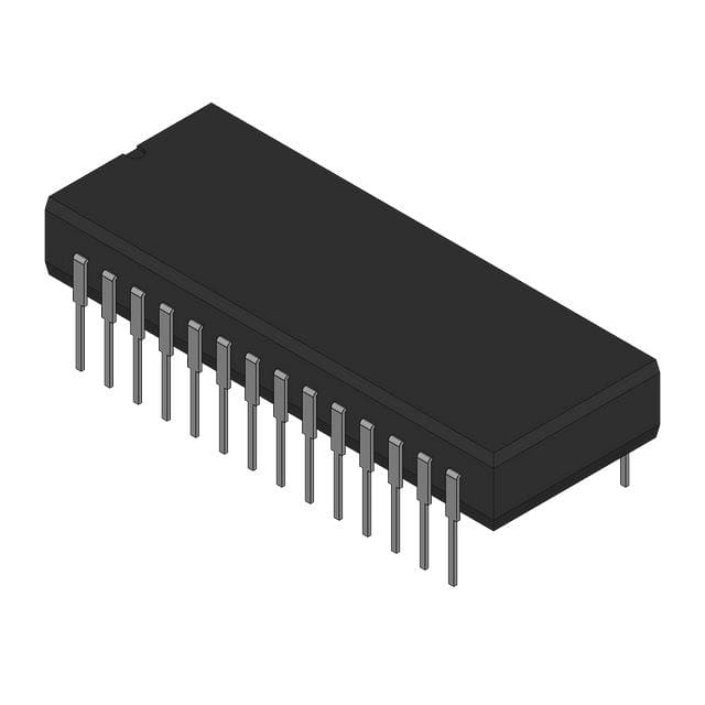
- Part No.:
- SN74ACT8997NT
- Manufacturer:
- Texas Instruments
- Category:
- Microprocessors
- Package:
- -
- Datasheet:
-
 SN74ACT8997NT.pdf
- Description:
- MICROPROCESSOR CIRCUIT PDIP28
- Quantity:
- Payment:

- Shipping:

Inventory:2,484
Please send an inquiry. Send us your inquiry, and we will respond immediately.
Product details
Overview
SN74ACT8997NT from Texas Instruments is a JTAG TAP concatenator IC that links up to four secondary scan paths into a primary IEEE 1149.1 test bus, featuring an 8-bit programmable up/down counter, 4-bit hardwired ID bus, TTL-compatible inputs, and EPIC 1-µm CMOS process technology - used in high-reliability board-level test infrastructure for complex digital systems.
For engineers reviewing the SN74ACT8997NT datasheet, SN74ACT8997NT pinout, SN74ACT8997NT application, or SN74ACT8997NT equivalent, this device supports scan-path partitioning, dynamic SSP selection via instruction-controlled registers, boundary-scan register access, IRERR detection, and configurable DCO output behavior - all critical for JTAG-based system testability architecture design and debug.
Technical Context
The SN74ACT8997NT implements a fully IEEE Std 1149.1-compliant TAP controller with six stable states and synchronous operation (except counter) on TCK rising edge. It integrates six data registers - bypass (1-bit), control (10-bit), counter (8-bit), boundary-scan (10-bit), ID-bus (4-bit), and select (8-bit) - each accessible via dedicated instructions loaded into its 8-bit instruction register.
Scan-path configuration is determined by decoding the 8-bit select register and 10-bit control register, enabling per-SSP DTMS routing, DTDO activation, and DCO source/polarity/drive mode selection. The 4-bit ID bus is hardwired and scanned via the ID-bus register, while the 8-bit counter operates asynchronously to DCI transitions and supports up/down counting with latch-on-zero and IRERR-triggered interrupt output.
Key Specifications
| Parameter | Value and Actual Design Meaning |
|---|---|
| Standard Compliance | Fully compliant with IEEE Std 1149.1-1990 (JTAG); includes TAP controller, IR, and six DRs. |
| Secondary Scan Paths | Supports up to four selectable secondary scan paths (SSP1–SSP4) via 8-bit select register. |
| Counter Function | 8-bit programmable up/down counter triggered by DCI transitions; outputs interrupt via DCO. |
| ID Bus | 4-bit hardwired identification bus (ID1–ID4), scanned via ID-bus register for subsystem identification. |
| Logic Family | TTL-compatible inputs; ACT (Advanced CMOS TTL) series with 5 V supply and EPIC 1-µm process. |
| Operating Temperature | 0°C to +70°C - specified for commercial-grade SN74ACT8997NT in 300-mil plastic DIP (NT) package. |
| Supply Voltage | VCC = 4.5 V to 5.5 V - ensures robust noise margin and compatibility with legacy 5 V test systems. |
Pinout & Package
SN74ACT8997NT is housed in a 300-mil 28-pin plastic dual in-line package (DIP), designated NT. Pin functions are electrically identical across DW, NT, and JT packages per TI SCAS157D datasheet.
| Pin/Terminal | Circuit Role | Design Meaning |
|---|---|---|
| TDI, TDO, TMS, TCK, TRST | JTAG Test Access Port (TAP) | IEEE 1149.1 mandatory interface; connects to primary scan chain; TDI/TDO shift IR/DR data serially. |
| DTDI1–DTDI4 | Secondary Scan Path Data Inputs | Receive TDO outputs from up to four downstream SSPs; internally pulled up when unconnected. |
| DTDO1–DTDO4 | Secondary Scan Path Data Outputs | Drive TDI inputs of selected SSPs; active only during Shift-IR/Shift-DR states per select register. |
| DTMS1–DTMS4 | Secondary Scan Path Mode Select | Route TMS or static logic level to selected SSPs; controlled by select register bit pairs (MSB/LSB). |
| DCI / DCO | Device Condition Interface | DCI accepts interrupt/protocol signals; DCO outputs counter overflow, IRERR, or DCI - configurable via control register. |
| ID1–ID4 | Subsystem Identification Bus | Hardwired 4-bit code scanned via ID-bus register; enables traceable identification of test domain. |
| MCI / MCO | Master Condition Interface | MCI receives protocol/interrupt from PBC; MCO relays to SSPs - decouples primary/secondary control domains. |
| GND / VCC | Power Supply | Single 5 V supply (4.5–5.5 V); GND reference for all I/O and internal logic; no separate analog/digital rails. |
Key Features
| Feature | Design Value |
|---|---|
| Configurable DCO Output | DCO can be set to output IRERR, counter zero flag (CE), DCI, or static level - with polarity, drive (open-drain/3-state), and enable control via 10-bit control register. |
| Dynamic SSP Selection | Any combination of up to four secondary scan paths can be included in the primary scan path using 8-bit select register - enabling flexible test partitioning without hardware changes. |
| Integrated Boundary-Scan Register | 10-bit BSR captures MCI/MCO/DCI status and supports EXTEST/INTEST/SAMPLE-PRELOAD - eliminating need for external boundary-scan logic at subsystem boundaries. |
| Programmable Counter Interrupt | 8-bit up/down counter triggers DCO on configurable DCI edge; latch-on-zero (count-down only) and parity-checked IRERR support deterministic interrupt generation. |
| TTL-Compatible Inputs | All inputs (TDI, TMS, TRST, DTDIx, IDx, DCI, MCI) meet TTL voltage thresholds - ensuring interoperability with legacy 5 V test controllers and logic families. |
Applications
| High-Density PCB Test Architecture | Modular System-on-Board Validation |
|---|---|
|
Use Scenario: Partitioning large ASIC/FPGA-based boards into independently testable subsystems using hierarchical JTAG chains. IC Role / Device Role / Timing Role: Acts as scan-path concatenator between primary test controller and four secondary scan domains; synchronizes TCK/IR/DR operations across domains. Use Value: Reduces test time by enabling parallel scan-path execution and eliminates manual jumpering or multiplexer switching during board bring-up. |
Use Scenario: Validating plug-in modules (e.g., memory, I/O, processor cards) in backplane-based systems before integration. IC Role / Device Role / Timing Role: Provides module-level ID-bus identification and SSP selection control - allowing test software to address specific modules within a shared JTAG daisy chain. Use Value: Enables automated module identification and targeted boundary-scan testing without physical reconfiguration or firmware updates. |
| Production Test Infrastructure | Field-Service Diagnostics |
|
Use Scenario: Embedding standardized test access in volume-manufactured telecom or industrial control boards requiring 100% test coverage. IC Role / Device Role / Timing Role: Serves as fixed-function test bridge with hardwired ID bus and programmable counter - supporting factory test scripts and failure logging via DCO interrupts. Use Value: Guarantees consistent test port behavior across production lots; eliminates dependency on programmable logic or microcontroller-based test agents. |
Use Scenario: Enabling technician-level diagnostics in deployed equipment using portable JTAG debuggers and minimal host software. IC Role / Device Role / Timing Role: Delivers subsystem identification (ID1–ID4), counter-triggered fault alerts (via DCO), and boundary-scan visibility - without requiring embedded firmware or OS support. Use Value: Allows rapid isolation of faulty modules or interconnects in the field using standard JTAG tools and preloaded test patterns. |
Equivalent & Alternatives
The following parts are listed as comparable options for similar JTAG TAP concatenation applications.
| Alternative Part | Technical Difference | Application Difference | Selection Advice |
|---|---|---|---|
| SN74ACT8996NT | 4-bit select capability only (no ID bus or counter); lacks DCO/DCI functionality and control register features. | Suitable for basic scan-path linking without subsystem identification or interrupt generation requirements. | Choose SN74ACT8996NT only if ID bus, counter, and DCO-driven diagnostics are unnecessary - reduces cost and complexity. |
| SN74ACT8998NT | Includes identical 4-bit ID bus and counter but adds 2-bit extended select register for eight SSPs and enhanced control register bits. | Required when more than four secondary scan paths must be managed in a single test domain. | Select SN74ACT8998NT when scaling beyond four SSPs or needing expanded control granularity - same pinout and voltage specs. |
Compared with SN74ACT8996NT and SN74ACT8998NT, the SN74ACT8997NT uniquely balances full IEEE 1149.1 compliance, 4-SSP support, integrated ID bus, and programmable counter - making it optimal for mid-complexity test architectures where identification and interrupt signaling are essential but eight-SSP scalability is not required.
Availability
SN74ACT8997NT is available at Aetrix Electronics and suitable for high-reliability PCB test infrastructure, modular system validation, and production-level JTAG diagnostics requiring stable component supply, long-lifecycle availability, and traceable sourcing.
Supply support for SN74ACT8997NT includes scheduled delivery planning, volume procurement assistance, BOM continuity management, traceable sourcing, and lifecycle availability coordination for OEM customers, industrial embedded developers, connected-device designers, and electronics production programs.
Manufacturer
Texas Instruments is a global semiconductor leader specializing in analog, embedded processing, and connectivity technologies, with decades of leadership in testability and JTAG solutions.
The SN74ACT8997NT belongs to TI's SCOPE™ family of testability ICs, designed specifically to simplify IEEE 1149.1 implementation in complex digital systems by providing configurable scan-path linking, subsystem identification, and hardware-assisted test control.
FAQ
What is the operating temperature range for the SN74ACT8997NT?
The SN74ACT8997NT is rated for commercial operation from 0°C to +70°C. This specification applies specifically to the NT-package variant; military-grade SN54ACT8997 devices operate from –55°C to +125°C but use different packaging (JT/FK). The SN74ACT8997NT's thermal rating aligns with standard industrial board-level test environments and ensures stable TAP controller timing and register behavior across its full range.
Does the SN74ACT8997NT support both up-counting and down-counting modes?
Yes, the SN74ACT8997NT supports both up-counting and down-counting via bit 9 of its 10-bit control register. When bit 9 = 0, the 8-bit counter increments on each DCI transition; when bit 9 = 1, it decrements. The counter operates asynchronously to DCI and can be configured to latch at zero (down-count only) using bit 8 - enabling precise event-triggered interrupt generation through DCO for diagnostic or synchronization use cases.
How is the 4-bit ID bus used in the SN74ACT8997NT?
The 4-bit ID bus (ID1–ID4) in the SN74ACT8997NT is hardwired to external pull-up/pull-down resistors to encode a fixed subsystem identification code. That code is scanned out via the ID-bus register (a subset of the 10-bit boundary-scan register) during normal JTAG operations. This allows test software to automatically detect and differentiate between multiple SN74ACT8997NT-equipped modules in a daisy-chained JTAG system without requiring configuration registers or firmware.
Can the SN74ACT8997NT be bypassed in a JTAG scan chain?
Yes, the SN74ACT8997NT supports IEEE 1149.1 BYPASS instruction (0x81, 0x84, etc.), which places its 1-bit bypass register between TDI and TDO. In bypass mode, the device presents minimal delay and does not load or shift data through its internal registers. This allows the primary scan chain to route around the SN74ACT8997NT when secondary scan paths are inactive or during initialization sequences - preserving chain integrity and timing predictability.
What are the key differences between SN74ACT8997NT and SN74ACT8996NT?
The SN74ACT8997NT includes a 4-bit ID bus, 8-bit programmable counter with DCO interrupt output, and full 10-bit control register - features absent in the SN74ACT8996NT. The latter supports only basic 4-SSP selection and lacks ID bus, counter, and advanced DCO configuration. Therefore, SN74ACT8997NT is required when subsystem identification, event counting, or hardware-triggered diagnostics are needed - while SN74ACT8996NT suffices for simple scan-path concatenation only.
SN74ACT8997NT Specifications
- Product attributes
- Attribute value
- Manufacturer:
- Texas Instruments
- Package/Case:
- -
- Series:
- *
- Packaging:
- Bulk
- Product Status:
- Active
- Core Processor:
- -
- Number of Cores/Bus Width:
- -
- Speed:
- -
- Co-Processors/DSP:
- -
- RAM Controllers:
- -
- Graphics Acceleration:
- -
- Display & Interface Controllers:
- -
- Ethernet:
- -
- SATA:
- -
- USB:
- -
- Voltage - I/O:
- -
- Operating Temperature:
- -
- Grade:
- -
- Qualification:
- -
- Security Features:
- -
- Mounting Type:
- -
- Supplier Device Package:
- -
- Additional Interfaces:
- -
SN74ACT8997NT FAQ
1.How can I place an order for SN74ACT8997NT through Aetrix?
Please submit a Request for Quotation (RFQ) for SN74ACT8997NT on Aetrix. Our sales agent will provide a competitive quotation and guide you through the order confirmation once you accept the terms.
2.Are the price and stock information for SN74ACT8997NT reliable?
The price and inventory of SN74ACT8997NT are updated periodically and may fluctuate due to market conditions. Stock and pricing data are typically refreshed every 24 hours. Quotation validity for SN74ACT8997NT is usually 5 days.
3.What payment methods are accepted for SN74ACT8997NT?
We accept Wire Transfer, PayPal, Credit Card, Western Union, MoneyGram, and Escrow for SN74ACT8997NT transactions.
Note: Certain payment methods may incur a processing fee.
4.How is shipping managed for SN74ACT8997NT?
SN74ACT8997NT orders can be shipped via leading logistics carriers, including DHL, UPS, FedEx, TNT, or Registered Mail.
Once your SN74ACT8997NT order is processed, you will receive an email with the shipment details and tracking number.
Note: Tracking information may take up to 24 hours to appear. Express delivery typically takes 3–5 business days.
5.How can I obtain technical support or documentation for SN74ACT8997NT?
For technical support, including SN74ACT8997NT datasheets, pinout diagrams, or application guidance, please contact our engineering support team. They can provide detailed documentation and assistance for your SN74ACT8997NT requirements.
6.How does Aetrix verify that SN74ACT8997NT is sourced from the original manufacturer or authorized distributors?
All SN74ACT8997NT products on Aetrix are procured from qualified distributors and authorized channels. Our dedicated quality assurance team conducts strict verification, including traceability checks and, if necessary, third-party testing. This ensures that SN74ACT8997NT meets industry standards.
7.What is the process for return or replacement of SN74ACT8997NT?
All SN74ACT8997NT units undergo pre-shipment inspection (PSI). If there is an issue with SN74ACT8997NT, returns or replacements are accepted under the following conditions:
1.Quantity discrepancies, incorrect items, or visible external defects (such as breakage or corrosion), acknowledged by Aetrix.
2.The issue is reported within 90 days of delivery.
3.The SN74ACT8997NT part is unused and in its original packaging.
Return procedure for SN74ACT8997NT:
1.Submit a request within 90 days.
2.Obtain a Return Material Authorization (RMA) from Aetrix.
SN74ACT8997NT Tags

-
AT91SAM9260B-CU-999
Microchip Technology
-
AT91SAM9G25-CU
Microchip Technology

-
ATSAMA5D27C-CU
Microchip Technology
-
AT91SAM9X35-CU
Microchip Technology
-
AT91SAM9X25-CU
Microchip Technology

-
MCIMX6Y2CVM08AB
NXP Semiconductors
.JPG)
-
AM3352BZCZ100
Texas Instruments
-
AT91SAM9260B-CU
Microchip Technology

-
AT91SAM9260B-QU
Microchip Technology

-
ATSAMA5D31A-CU
Microchip Technology
-
AT91SAM9G20B-CU-999
Microchip Technology
-
MCIMX6Y2CVM05AB
NXP Semiconductors
Tech Hub

A practical engineering guide to 3.3V and 5V logic compatibility, input thresholds, resistor dividers, translator ICs, MOSFET level shifting, I2C pull-ups, timing limits and power-sequencing risks.

The 74HC595 uses push-pull logic outputs, while the TPIC6B595 uses 50 V open-drain DMOS sinks for higher-power loads. This guide compares timing, current limits, 3.3 V interfacing, load wiring, thermal…

The 74HC595 converts serial data into eight stable parallel outputs. This guide covers pin functions, shift and storage timing, OE and MR behavior, drive-current limits, cascading, voltage compatibilit…

A technical comparison of level-sensitive latches and edge-triggered flip-flops, covering timing windows, setup and hold limits, master–slave operation, time borrowing, race-through, HDL inference and…

A D latch stores one bit while Enable controls when data can pass. This reference covers gate-level operation, truth tables, transparency, setup and hold timing, LE versus OE, common ICs and practical …

An SR latch stores one bit through cross-coupled feedback. This engineering reference covers NOR and NAND implementations, truth tables, forbidden-state recovery, gated operation, switch debouncing, fa…

Latch circuits retain one bit through feedback. This technical reference covers SR and D latches, truth tables, transparency, timing limits, latch-versus-flip-flop behavior, applications and common log…

An engineering guide to LED driver operation, constant-current and constant-voltage outputs, linear and switching topologies, dimming, IC selection, calculations, replacement compatibility, and fault c…

Operational amplifier guide covering op amp basics, feedback, ideal vs real op amps, common configurations, buffer circuits, offset, bias current, gain-bandwidth, slew rate, rail-to-rail limits and sel…

Jumper cables guide covering safe connection order, red and black clamp placement, final ground connection, cable gauge, length, clamp quality, copper vs CCA cables, jump starter comparison and battery…


