
 My Inquiry
 My Account


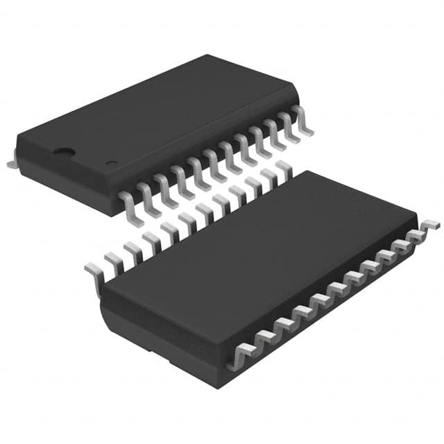
Texas Instruments SN74GTLPH306DWR
- Part No.:
- SN74GTLPH306DWR
- Manufacturer:
- Texas Instruments
- Category:
- Translators, Level Shifters
- Package:
- Datasheet:
-
 SN74GTLPH306DWR.pdf
- Description:
- IC TRANSLTR BIDIRECTIONAL 24SOIC
- Quantity:
- Payment:

- Shipping:

Inventory:3,898
Please send an inquiry. Send us your inquiry, and we will respond immediately.
Product details
Overview
SN74GTLPH306DWR from Texas Instruments is an 8-bit bidirectional LVTTL-to-GTLP bus transceiver in SOIC-24 package, supporting hot insertion via Ioff and power-up 3-state, with 5-V-tolerant A-port inputs, 50 mA GTLP B-port drive, and TI-OPC/OEC circuitry for backplane signal integrity. It enables high-speed communication between LVTTL logic cards and GTLP backplanes in telecom switching systems.
For engineers reviewing the SN74GTLPH306DWR datasheet, SN74GTLPH306DWR pinout, SN74GTLPH306DWR application, or SN74GTLPH306DWR equivalent, key selection considerations include GTLP/LVTTL level translation capability, 24-pin SOIC mechanical compatibility, distributed-load timing performance (tPLH = 3.6 ns into RLC load), bus-hold on A inputs, and VREF-referenced differential B-port interface.
Technical Context
The SN74GTLPH306DWR implements asynchronous bidirectional data flow controlled by DIR and OE pins, with noninverting polarity and independent A→B and B→A paths. Its TI-OPC circuitry actively limits overshoot during low-to-high transitions on unevenly loaded backplanes, while OEC circuitry reduces EMI and improves settling time.
It supports dual-mode operation at GTL (VTT = 1.2 V, VREF = 0.8 V) or GTLP (VTT = 1.5 V, VREF = 1 V) signal levels, with A-port inputs tolerant to 5 V and compatible with TTL/CMOS, and B-port inputs referenced to VREF. The device achieves incident-wave switching down to 19 Ω load impedance using medium-drive GTLP outputs.
Key Specifications
| Parameter | Value and Actual Design Meaning |
|---|---|
| VCC supply | 3.15–3.45 V - ensures stable operation within standard 3.3-V rail tolerances |
| GTLP output drive | 50 mA - enables reliable signaling into heavily loaded backplanes with ≤19 Ω impedance |
| LVTTL output drive | –24 mA / 24 mA - supports standard LVTTL fanout without external buffers |
| Propagation delay (A→B, RLC load) | tPLH = 3.6 ns - optimized for high-speed distributed backplane timing |
| Bus-hold current (A port) | IBHL = 75 µA - maintains valid logic state on unused LVTTL inputs without pull resistors |
| Hot-insertion support | Ioff ≤ 10 µA at VCC = 0 - prevents backflow current during live card insertion |
| Rise/fall time (B outputs) | tr = 1.2 ns, tf = 2.2 ns - balances speed and signal integrity for GTLP compliance |
Pinout & Package
SN74GTLPH306DWR uses a 24-pin SOIC (DW) package with 0.65 mm pitch, 7.5 mm × 15.4 mm body, and 1.2 mm max height per JEDEC MO-153. Pin 1 index is located at top-left corner of the package marking side.
| Pin/Terminal | Circuit Role | Design Meaning |
|---|---|---|
| 1, 6, 11, 14, 19, 22 | GND | Ground reference for both A and B ports; six dedicated ground pins reduce noise coupling |
| 2 | VCC | Main 3.3-V supply for internal logic and A-port drivers |
| 3–10 | A1–A8 | LVTTL-compatible data inputs/outputs (5-V tolerant); feature bus-hold circuitry |
| 12 | DIR | Direction control: high enables A→B, low enables B→A data flow |
| 13 | VREF | Differential reference voltage input for B-port receivers; sets GTLP input threshold |
| 15–22 | B1–B8 | GTLP-level data inputs/outputs; terminated to VTT (1.5 V) for proper signaling |
| 23 | OE | Output enable: low activates transceiver, high places all outputs in high-Z state |
| 24 | OE | Output enable: low activates transceiver, high places all outputs in high-Z state |
Key Features
| Feature | Design Value |
|---|---|
| TI-OPC active overshoot control | Minimizes ringing on unevenly loaded backplanes during low-to-high transitions, preserving noise margin at >100 MHz |
| OEC signal integrity enhancement | Reduces EMI and shortens bus settling time through optimized driver/receiver architecture |
| 5-V-tolerant LVTTL I/O | Allows direct interfacing with legacy 5-V TTL and CMOS logic without level-shifting components |
| Integrated bus-hold on A inputs | Eliminates need for external pullup/pulldown resistors on undriven A-port lines |
| Hot-insertion support | Ioff ≤ 10 µA and power-up 3-state ensure safe insertion into live backplanes without disrupting system operation |
Applications
| Telecom Backplane Interfacing | Industrial Control Backplanes |
|---|---|
|
Use Scenario: High-speed data routing between line cards and switch fabric in modular telecom chassis. IC Role / Device Role / Timing Role: Level-translating bus transceiver enabling LVTTL-based control cards to communicate with GTLP-terminated backplane infrastructure. Use Value: Enables three-times-faster backplane operation vs. standard LVTTL, with TI-OPC maintaining signal integrity across variable slot loading. |
Use Scenario: Distributed I/O module interconnection in programmable logic controller (PLC) racks with mixed-voltage subsystems. IC Role / Device Role / Timing Role: Bidirectional protocol-agnostic bridge between 3.3-V LVTTL CPU modules and GTLP-specified fieldbus backplanes. Use Value: Provides hot-plug capability and bus-hold protection for maintenance without system shutdown, reducing downtime. |
| Test Equipment Backplane | High-Density Data Acquisition Systems |
|
Use Scenario: Signal conditioning and multiplexing in automated test equipment (ATE) mainframes with modular instrument slots. IC Role / Device Role / Timing Role: GTLP transceiver isolating LVTTL host controller from high-speed measurement data lanes on shared backplane. Use Value: Delivers sub-4 ns propagation delay into distributed RLC loads, meeting tight timing budgets for synchronized sampling. |
Use Scenario: Sensor data aggregation across multiple analog front-end modules in precision instrumentation racks. IC Role / Device Role / Timing Role: Level-shifting transceiver linking LVTTL-configured FPGA controllers to GTLP-optimized data concentrator backplanes. Use Value: Supports incident-wave switching into 19 Ω loads, enabling deterministic latency for time-critical acquisition triggers. |
Equivalent & Alternatives
The following parts are listed as comparable options for similar bus transceiver applications.
| Alternative Part | Technical Difference | Application Difference | Selection Advice |
|---|---|---|---|
| SN74GTLPH16306DGVR | 16-bit version in TVSOP-48 package; identical GTLP/LVTTL translation architecture and TI-OPC/OEC features | Requires PCB redesign due to doubled pin count and different footprint; suited for wider data buses | Select when 16-bit width is required and board layout allows TVSOP-48 placement |
| SN74GTLPH305DWR | 8-bit unidirectional GTLP transceiver (A→B only); lacks DIR pin and B→A path; same SOIC-24 package | Cannot support bidirectional protocols like JTAG or shared-memory arbitration without additional logic | Choose only for fixed-direction backplane links where cost and simplicity outweigh flexibility needs |
Compared with SN74GTLPH306DWR, SN74GTLPH16306DGVR doubles data width but increases board area and power, while SN74GTLPH305DWR sacrifices bidirectionality for lower gate count and cost-neither offers pin compatibility or drop-in replacement capability.
Availability
SN74GTLPH306DWR is available at Aetrix Electronics and suitable for telecom backplane interfacing, industrial control backplanes, and test equipment backplane applications requiring stable component supply, long-term lifecycle support, and traceable sourcing.
Supply support for SN74GTLPH306DWR includes scheduled delivery planning, volume procurement assistance, BOM continuity management, traceable sourcing, and lifecycle availability coordination for OEM customers, industrial embedded developers, connected-device designers, and electronics production programs.
Manufacturer
Texas Instruments is a global semiconductor leader specializing in analog, embedded processing, and logic solutions, with over 50 years of innovation in high-speed interface ICs.
The SN74GTLPH306DWR belongs to TI's GTLP logic family, designed specifically for high-speed, noise-resilient backplane communication in telecom, industrial, and test equipment systems requiring robust level translation and hot-insertion reliability.
FAQ
What is the primary function of the SN74GTLPH306DWR?
The SN74GTLPH306DWR is an 8-bit bidirectional bus transceiver that translates signal levels between LVTTL (3.3 V logic with 5-V tolerance) on the A port and GTLP (1.5 V termination) on the B port. It enables high-speed, low-noise communication across backplanes in telecom and industrial systems, with built-in TI-OPC and OEC circuitry for signal integrity.
Does the SN74GTLPH306DWR support hot insertion?
Yes, the SN74GTLPH306DWR supports hot insertion via two integrated features: Ioff circuitry limits current backflow when VCC = 0 (≤10 µA), and power-up 3-state ensures all outputs remain high-impedance during power ramp-up. These features protect the device and backplane during live card replacement in systems like telecom chassis.
What are the recommended operating conditions for VREF and VTT on the SN74GTLPH306DWR?
For GTLP mode, the SN74GTLPH306DWR requires VTT = 1.35–1.65 V (nominal 1.5 V) and VREF = 0.87–1.1 V (nominal 1 V). VREF must be set within 0.6 V of VTT to minimize current drain, and TI-OPC activates when VTT exceeds VREF by >0.7 V. Operation at GTL levels (VTT = 1.2 V, VREF = 0.8 V) is also supported.
Can the SN74GTLPH306DWR be used with standard TTL logic?
Yes, the A-port inputs and control pins of the SN74GTLPH306DWR are 5-V tolerant and compatible with standard TTL and 5-V CMOS logic families. This allows direct connection to legacy 5-V controllers without external level shifters, while the B port remains strictly GTLP-compliant with VTT = 1.5 V termination.
What is the significance of the bus-hold feature on the A-port inputs of the SN74GTLPH306DWR?
The bus-hold circuitry on the A-port inputs of the SN74GTLPH306DWR actively maintains a valid logic state (high or low) on undriven or floating inputs, eliminating the need for external pullup or pulldown resistors. It sources/sinks ≥75 µA to sustain logic levels, improving system reliability in modular backplane designs with variable slot occupancy.
SN74GTLPH306DWR Specifications
- Product attributes
- Attribute value
- Manufacturer:
- Texas Instruments
- Series:
- 74GTLPH
- Package/Case:
- Packaging:
- Tape & Reel (TR)
- Product Status:
- Active
- Translator Type:
- Mixed Signal
- Channel Type:
- Bidirectional
- Number of Circuits:
- 1
- Channels per Circuit:
- 8
- Voltage - VCCA:
- -
- Voltage - VCCB:
- -
- Input Signal:
- LVTTL
- Output Signal:
- GTLP
- Output Type:
- Tri-State, Non-Inverted
- Data Rate:
- -
- Operating Temperature:
- -40°C ~ 85°C (TA)
- Grade:
- -
- Qualification:
- -
- Features:
- -
- Mounting Type:
- Surface Mount
- Supplier Device Package:
- 24-SOIC (0.295", 7.50mm Width)
SN74GTLPH306DWR FAQ
1.How can I place an order for SN74GTLPH306DWR through Aetrix?
Please submit a Request for Quotation (RFQ) for SN74GTLPH306DWR on Aetrix. Our sales agent will provide a competitive quotation and guide you through the order confirmation once you accept the terms.
2.Are the price and stock information for SN74GTLPH306DWR reliable?
The price and inventory of SN74GTLPH306DWR are updated periodically and may fluctuate due to market conditions. Stock and pricing data are typically refreshed every 24 hours. Quotation validity for SN74GTLPH306DWR is usually 5 days.
3.What payment methods are accepted for SN74GTLPH306DWR?
We accept Wire Transfer, PayPal, Credit Card, Western Union, MoneyGram, and Escrow for SN74GTLPH306DWR transactions.
Note: Certain payment methods may incur a processing fee.
4.How is shipping managed for SN74GTLPH306DWR?
SN74GTLPH306DWR orders can be shipped via leading logistics carriers, including DHL, UPS, FedEx, TNT, or Registered Mail.
Once your SN74GTLPH306DWR order is processed, you will receive an email with the shipment details and tracking number.
Note: Tracking information may take up to 24 hours to appear. Express delivery typically takes 3–5 business days.
5.How can I obtain technical support or documentation for SN74GTLPH306DWR?
For technical support, including SN74GTLPH306DWR datasheets, pinout diagrams, or application guidance, please contact our engineering support team. They can provide detailed documentation and assistance for your SN74GTLPH306DWR requirements.
6.How does Aetrix verify that SN74GTLPH306DWR is sourced from the original manufacturer or authorized distributors?
All SN74GTLPH306DWR products on Aetrix are procured from qualified distributors and authorized channels. Our dedicated quality assurance team conducts strict verification, including traceability checks and, if necessary, third-party testing. This ensures that SN74GTLPH306DWR meets industry standards.
7.What is the process for return or replacement of SN74GTLPH306DWR?
All SN74GTLPH306DWR units undergo pre-shipment inspection (PSI). If there is an issue with SN74GTLPH306DWR, returns or replacements are accepted under the following conditions:
1.Quantity discrepancies, incorrect items, or visible external defects (such as breakage or corrosion), acknowledged by Aetrix.
2.The issue is reported within 90 days of delivery.
3.The SN74GTLPH306DWR part is unused and in its original packaging.
Return procedure for SN74GTLPH306DWR:
1.Submit a request within 90 days.
2.Obtain a Return Material Authorization (RMA) from Aetrix.
SN74GTLPH306DWR Tags
-
74LVC1T45GW,125
Nexperia USA Inc.
-
74LVCH2T45DC,125
Nexperia USA Inc.

-
SN74LVC1T45DBVR
Texas Instruments
-
SN74LVC1T45DRLR
Texas Instruments
-
SN74LVC1T45DPKR
Texas Instruments
-
SN74LVC2T45DCTR
Texas Instruments
-
74LVC2T45GT,115
Nexperia USA Inc.
-
SN74LVC1T45YZPR
Texas Instruments

-
LSF0102DCUR
Texas Instruments

-
SN74LVC1T45DCKR
Texas Instruments
-
TXS0102DCTR
Texas Instruments
-
FXLP34P5X
onsemi
Tech Hub

A practical engineering guide to 3.3V and 5V logic compatibility, input thresholds, resistor dividers, translator ICs, MOSFET level shifting, I2C pull-ups, timing limits and power-sequencing risks.

The 74HC595 uses push-pull logic outputs, while the TPIC6B595 uses 50 V open-drain DMOS sinks for higher-power loads. This guide compares timing, current limits, 3.3 V interfacing, load wiring, thermal…

The 74HC595 converts serial data into eight stable parallel outputs. This guide covers pin functions, shift and storage timing, OE and MR behavior, drive-current limits, cascading, voltage compatibilit…

A technical comparison of level-sensitive latches and edge-triggered flip-flops, covering timing windows, setup and hold limits, master–slave operation, time borrowing, race-through, HDL inference and…

A D latch stores one bit while Enable controls when data can pass. This reference covers gate-level operation, truth tables, transparency, setup and hold timing, LE versus OE, common ICs and practical …

An SR latch stores one bit through cross-coupled feedback. This engineering reference covers NOR and NAND implementations, truth tables, forbidden-state recovery, gated operation, switch debouncing, fa…

Latch circuits retain one bit through feedback. This technical reference covers SR and D latches, truth tables, transparency, timing limits, latch-versus-flip-flop behavior, applications and common log…

An engineering guide to LED driver operation, constant-current and constant-voltage outputs, linear and switching topologies, dimming, IC selection, calculations, replacement compatibility, and fault c…

Operational amplifier guide covering op amp basics, feedback, ideal vs real op amps, common configurations, buffer circuits, offset, bias current, gain-bandwidth, slew rate, rail-to-rail limits and sel…

Jumper cables guide covering safe connection order, red and black clamp placement, final ground connection, cable gauge, length, clamp quality, copper vs CCA cables, jump starter comparison and battery…


