
 My Inquiry
 My Account


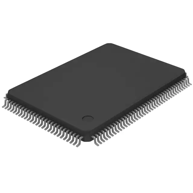
Texas Instruments SN74V3640-15PEU
- Part No.:
- SN74V3640-15PEU
- Manufacturer:
- Texas Instruments
- Category:
- FIFOs Memory
- Package:
- 128-LQFP
- Datasheet:
-
 SN74V3640-15PEU.pdf
- Description:
- IC FIFO SYNC 1KX36 10NS 128LQFP
- Quantity:
- Payment:

- Shipping:

Inventory:2,475
Please send an inquiry. Send us your inquiry, and we will respond immediately.
Product details
Overview
SN74V3640-15PEU from Texas Instruments is a 3.3-V CMOS, 1024 × 36-bit synchronous FIFO memory with independent read/write clocks, user-selectable bus sizing (×36/×18/×9), and first-word fall-through (FWFT) or standard timing mode. It delivers 166-MHz operation (6-ns read/write cycle time), zero-latency retransmit capability, and 5-V-tolerant inputs - deployed in high-speed network packet buffering and video data stream alignment.
For engineers reviewing the SN74V3640-15PEU datasheet, SN74V3640-15PEU pinout, SN74V3640-15PEU application, or SN74V3640-15PEU equivalent, key selection considerations include configurable bus-matching width, programmable almost-empty/almost-full flag offsets, big-endian/little-endian byte ordering, dual-clock domain operation, and TQFP-128 packaging for dense PCB layouts.
Technical Context
This FIFO implements a dual-clock, asynchronous read/write architecture with fully independent WCLK and RCLK domains (0–166 MHz), enabling seamless bridging between mismatched data rates in telecom and signal processing systems. Its RAM array supports flexible port sizing via BM/IW/OW control pins during master reset, and its flag logic includes EF/OR, FF/IR, HF, PAE, and PAF with selectable synchronous/asynchronous timing modes.
The device features fixed low-latency first-word access (three RCLK edges in FWFT mode), zero-latency retransmit (enabled by RM pin), and serial/parallel offset programming of PAE/PAF thresholds using LD/FSEL0/FSEL1. Bus-matching configuration preserves data integrity across ×36-to-×9 width conversions while maintaining consistent word alignment via BE-controlled endian selection.
Key Specifications
| Parameter | Value and Actual Design Meaning |
|---|---|
| Memory Depth × Width | 1024 × 36 bits - provides 36.9 kbit buffer capacity for burst-mode data staging without external memory management logic. |
| Max Clock Frequency | 166 MHz - enables 6-ns read/write cycle time, supporting high-throughput interfaces such as PCI-X and parallel video streams. |
| Bus Configuration | ×36/×18/×9 input and output ports - allows dynamic width adaptation (e.g., ×36-in to ×9-out) using BM/IW/OW pins at reset. |
| Timing Mode | FWFT or standard mode - selected by FWFT/SI pin at master reset; FWFT delivers immediate first-word visibility without REN assertion. |
| Flag Programmability | PAE and PAF with eight default offsets or custom values - programmed serially (via FWFT/SI) or in parallel (via Dn) for precise buffer-level monitoring. |
| Input Voltage Tolerance | 5-V-tolerant inputs - permits direct interfacing with legacy 5-V logic without level-shifting circuitry on control/data lines. |
| Retransmit Latency | Zero-latency option - enabled by RM pin during MRS; places first retransmitted word on Qn synchronously with initiating RCLK edge. |
Pinout & Package
SN74V3640-15PEU is housed in a 128-pin Thin Quad Flat Pack (TQFP) package with 0.4-mm lead pitch and exposed thermal pad. Pin assignments are validated per TI SCAS668A datasheet Figure 2 (PEU top view).
| Pin/Terminal | Circuit Role | Design Meaning |
|---|---|---|
| D0–D35 | Data input bus | 36-bit parallel input port; unused pins float in ×18/×9 modes - supports configurable write-port width under BM/IW control. |
| Q0–Q35 | Data output bus | 36-bit parallel output port; high-impedance when OE = high - retains last valid data when REN inactive in standard mode. |
| WCLK / RCLK | Independent clock inputs | Asynchronous domain clocks (0–166 MHz); no frequency ratio constraints - enables rate-matching between source/sink subsystems. |
| WEN / REN / OE | Enable controls | Edge-triggered write/read gating and 3-state output control - all active-low; OE overrides Qn state regardless of REN/WEN status. |
| MRS / PRS | Reset inputs | MRS initializes pointers, flags, and configuration; PRS resets pointers only - preserves FWFT mode, flag offsets, and endian setting. |
| EF/OR / FF/IR / HF | Status flags | Dual-function flags: EF/FF in standard mode; OR/IR in FWFT mode; HF always indicates ≥512 words stored - used for flow control handshake. |
| PAE / PAF | Programmable threshold flags | Assert at user-defined fill levels (e.g., 8/16/32 words); timing mode (sync/async) set by PFM pin - enables adaptive buffer management. |
| BM / IW / OW / BE | Configuration inputs | Set during master reset only - define bus width mapping, byte order (MSB-first vs LSB-first), and parity handling for offset programming. |
Key Features
| Feature | Design Value |
|---|---|
| First-word fall-through (FWFT) mode | Delivers first written word to outputs after exactly three RCLK edges - eliminates REN dependency for initial read, reducing latency in streaming pipelines. |
| Zero-latency retransmit | Places retransmitted first word on Qn within same RCLK cycle that RT is asserted - critical for real-time retry protocols without pipeline stall. |
| Flexible bus-matching | Supports five bidirectional width combinations (e.g., ×36→×9, ×9→×36) via static BM/IW/OW pins - avoids glue logic in heterogeneous interface bridging. |
| Big-/little-endian byte ordering | Configurable MSB-first or LSB-first word assembly during width conversion - ensures correct data interpretation when crossing 32-bit/16-bit/8-bit boundaries. |
| 5-V-tolerant inputs | Accepts 0–5.5 V on all control and data inputs while operating at 3.3 V VCC - simplifies mixed-voltage system integration without external translators. |
| Independent flag timing modes | PAE/PAF can operate synchronously (edge-aligned to RCLK/WCLK) or asynchronously (level-sensitive) - selected by PFM pin at reset for deterministic timing closure. |
Applications
| Network Packet Buffering | Video Data Stream Alignment |
|---|---|
|
Use Scenario: Staging Ethernet frames between MAC and PHY layers with variable inter-packet gaps and bursty traffic patterns. IC Role / Device Role / Timing Role: Synchronous FIFO buffer with independent WCLK/RCLK domains absorbing jitter and rate mismatches between 100-Mbps MAC and 1-Gbps PHY. Use Value: FWFT mode ensures immediate frame availability upon arrival; programmable PAF triggers DMA fetch before overflow, sustaining 166-MHz throughput. |
Use Scenario: Aligning parallel RGB/YUV pixel streams from image sensor to display controller with differing clock domains and blanking intervals. IC Role / Device Role / Timing Role: Dual-clock FIFO providing elastic storage for horizontal line buffering and vertical scaling synchronization. Use Value: ×36-in to ×18-out bus matching adapts 36-bit sensor output to 18-bit display interface; BE pin configures MSB-aligned pixel packing. |
| Telecom Line Card Bridging | Signal Processing Data Pipelining |
|
Use Scenario: Interfacing TDM backplane (E1/T1) with packet-switched core using HDLC framing and CRC insertion. IC Role / Device Role / Timing Role: High-density FIFO decoupling fixed-rate serial line interface from variable-latency packet processor. Use Value: 1024-word depth accommodates worst-case HDLC frame + overhead; zero-latency retransmit enables rapid CRC recalculation on corrupted frames. |
Use Scenario: Feeding multi-stage DSP algorithms (FFT → filtering → modulation) where each stage operates at different clock frequencies. IC Role / Device Role / Timing Role: Clock-domain crossing FIFO ensuring deterministic data handoff between asynchronous processing blocks. Use Value: Independent WCLK/RCLK allow 125-MHz FFT engine to feed 80-MHz filter bank; PAE/PAF flags trigger stage activation at optimal buffer occupancy. |
Equivalent & Alternatives
The following parts are listed as comparable options for similar FIFO memory applications.
| Alternative Part | Technical Difference | Application Difference | Selection Advice |
|---|---|---|---|
| IDT72V3640L15PF | Same 1024 × 36 organization and 166-MHz speed, but uses 3.3-V LVTTL I/O (not 5-V tolerant) and lacks FWFT mode - requires external logic for first-word visibility. | Best suited for fully 3.3-V systems with tight timing budgets where FWFT is unnecessary and board space permits added control logic. | Select IDT72V3640L15PF only if 5-V tolerance is irrelevant and FWFT functionality is not required in your data path. |
| ON Semiconductor NB3N502M | Smaller 512 × 18 capacity, 133-MHz max speed, and no programmable flags - offers integrated PLL but lacks bus-matching flexibility and retransmit capability. | Ideal for compact clock-synchronized buffers in consumer audio/video SoC interfaces where depth and configurability are secondary to integration. | Choose NB3N502M for cost-sensitive, space-constrained designs needing basic FIFO + clock synthesis - not for high-depth, multi-width, or retransmit-critical use cases. |
Compared with IDT72V3640L15PF and NB3N502M, SN74V3640-15PEU uniquely combines 5-V-tolerant I/O, FWFT timing, zero-latency retransmit, and full ×36/×18/×9 bus-matching - making it the only option supporting robust interoperability across legacy and modern voltage domains while enabling latency-optimized streaming architectures.
Availability
SN74V3640-15PEU is available at Aetrix Electronics and suitable for network packet buffering, video stream alignment, telecom line card bridging, signal processing pipelining, and high-speed data acquisition requiring stable component supply across extended production cycles.
Supply support for SN74V3640-15PEU includes scheduled delivery planning, volume procurement assistance, BOM continuity management, traceable sourcing, and lifecycle availability coordination for OEM customers, industrial embedded developers, connected-device designers, and electronics production programs.
Manufacturer
Texas Instruments is a global semiconductor leader specializing in analog, embedded processing, and logic solutions, with over 50 years of innovation in high-reliability interface and memory products.
SN74V3640-15PEU belongs to TI's high-speed synchronous FIFO product line, engineered specifically for deterministic, low-latency data buffering in multi-clock-domain systems such as networking infrastructure, broadcast video equipment, and telecom base stations.
FAQ
What is the maximum operating frequency of the SN74V3640-15PEU?
The SN74V3640-15PEU supports up to 166 MHz for both read and write operations, corresponding to a 6-ns read/write cycle time. This specification is guaranteed across the commercial temperature range (0°C to 70°C) and applies to both WCLK and RCLK domains independently - enabling high-throughput data transfer in demanding applications like packet switching and real-time video processing. The SN74V3640-15PEU achieves this performance using submicron CMOS technology optimized for speed and low power.
Does the SN74V3640-15PEU support 5-V logic inputs?
Yes, the SN74V3640-15PEU features 5-V-tolerant inputs on all control and data pins (D0–D35, WEN, REN, MRS, etc.), allowing direct connection to 5-V TTL or CMOS logic without external level shifters. This tolerance holds across the full operating voltage range (3.0 V to 3.6 V VCC) and is specified in the absolute maximum ratings and DC characteristics sections of the TI SCAS668A datasheet. The SN74V3640-15PEU maintains full functionality and timing compliance under 5-V input conditions.
How does the first-word fall-through (FWFT) mode work on the SN74V3640-15PEU?
In FWFT mode - selected by asserting FWFT/SI high during master reset - the first word written to an empty SN74V3640-15PEU appears on Q0–Q35 after exactly three rising edges of RCLK, without requiring REN to be asserted. Subsequent words still require REN activation. This behavior eliminates initial read latency in streaming applications. The SN74V3640-15PEU uses OR and IR flags instead of EF/FF in FWFT mode to indicate output readiness and input space availability.
Can the SN74V3640-15PEU be configured for different input and output bus widths?
Yes, the SN74V3640-15PEU supports five bus-matching configurations (e.g., ×36-in to ×9-out) via BM, IW, and OW pins sampled during master reset. These pins define write-port and read-port widths independently, enabling seamless interface translation between mismatched subsystems. The SN74V3640-15PEU maintains data coherency across width changes using BE-controlled endian selection and automatic bit alignment - no external multiplexing logic is needed.
What is the purpose of the programmable almost-empty (PAE) and almost-full (PAF) flags on the SN74V3640-15PEU?
The PAE and PAF flags on the SN74V3640-15PEU provide early warning signals at user-defined buffer occupancy thresholds - configurable via eight factory defaults or custom values loaded serially (FWFT/SI) or in parallel (Dn). PAE asserts when word count falls below a set value; PAF asserts when free space drops below a threshold. These flags enable proactive DMA triggering, flow control negotiation, or resource allocation in real-time systems - a capability not available in basic FIFOs. The SN74V3640-15PEU supports synchronous or asynchronous timing modes for these flags via the PFM pin.
SN74V3640-15PEU Specifications
- Product attributes
- Attribute value
- Manufacturer:
- Texas Instruments
- Series:
- 74V
- Package/Case:
- 128-LQFP
- Packaging:
- Tray
- Product Status:
- Obsolete
- Programmable:
- Not Verified
- Memory Size:
- 36K (1K x 36)
- Function:
- Synchronous
- Data Rate:
- 66.7MHz
- Access Time:
- 10ns
- Voltage - Supply:
- 3.15 V ~ 3.45 V
- Current - Supply (Max):
- 40mA
- Bus Directional:
- Uni-Directional
- Expansion Type:
- Depth, Width
- Programmable Flags Support:
- Yes
- Retransmit Capability:
- Yes
- FWFT Support:
- Yes
- Operating Temperature:
- 0°C ~ 70°C
- Mounting Type:
- Surface Mount
- Supplier Device Package:
- 128-LQFP (20x14)
SN74V3640-15PEU FAQ
1.How can I place an order for SN74V3640-15PEU through Aetrix?
Please submit a Request for Quotation (RFQ) for SN74V3640-15PEU on Aetrix. Our sales agent will provide a competitive quotation and guide you through the order confirmation once you accept the terms.
2.Are the price and stock information for SN74V3640-15PEU reliable?
The price and inventory of SN74V3640-15PEU are updated periodically and may fluctuate due to market conditions. Stock and pricing data are typically refreshed every 24 hours. Quotation validity for SN74V3640-15PEU is usually 5 days.
3.What payment methods are accepted for SN74V3640-15PEU?
We accept Wire Transfer, PayPal, Credit Card, Western Union, MoneyGram, and Escrow for SN74V3640-15PEU transactions.
Note: Certain payment methods may incur a processing fee.
4.How is shipping managed for SN74V3640-15PEU?
SN74V3640-15PEU orders can be shipped via leading logistics carriers, including DHL, UPS, FedEx, TNT, or Registered Mail.
Once your SN74V3640-15PEU order is processed, you will receive an email with the shipment details and tracking number.
Note: Tracking information may take up to 24 hours to appear. Express delivery typically takes 3–5 business days.
5.How can I obtain technical support or documentation for SN74V3640-15PEU?
For technical support, including SN74V3640-15PEU datasheets, pinout diagrams, or application guidance, please contact our engineering support team. They can provide detailed documentation and assistance for your SN74V3640-15PEU requirements.
6.How does Aetrix verify that SN74V3640-15PEU is sourced from the original manufacturer or authorized distributors?
All SN74V3640-15PEU products on Aetrix are procured from qualified distributors and authorized channels. Our dedicated quality assurance team conducts strict verification, including traceability checks and, if necessary, third-party testing. This ensures that SN74V3640-15PEU meets industry standards.
7.What is the process for return or replacement of SN74V3640-15PEU?
All SN74V3640-15PEU units undergo pre-shipment inspection (PSI). If there is an issue with SN74V3640-15PEU, returns or replacements are accepted under the following conditions:
1.Quantity discrepancies, incorrect items, or visible external defects (such as breakage or corrosion), acknowledged by Aetrix.
2.The issue is reported within 90 days of delivery.
3.The SN74V3640-15PEU part is unused and in its original packaging.
Return procedure for SN74V3640-15PEU:
1.Submit a request within 90 days.
2.Obtain a Return Material Authorization (RMA) from Aetrix.
SN74V3640-15PEU Tags
-
7201LA15JGI
Renesas
-
7204L12JG
Renesas

-
72V82L15PAG8
Renesas

-
7205L15JGI
Renesas
-
7208L20JG
Renesas

-
72V2105L10PFG
Renesas
-
72V2111L15PFGI
Renesas

-
72V2113L6PFG
Renesas
-
72V36110L6PFG
Renesas

-
SN74ALVC7804-40DL
Texas Instruments
-
7202LA25JGI
Renesas
-
SN74V245-15PAG
Texas Instruments
Tech Hub

A practical engineering guide to 3.3V and 5V logic compatibility, input thresholds, resistor dividers, translator ICs, MOSFET level shifting, I2C pull-ups, timing limits and power-sequencing risks.

The 74HC595 uses push-pull logic outputs, while the TPIC6B595 uses 50 V open-drain DMOS sinks for higher-power loads. This guide compares timing, current limits, 3.3 V interfacing, load wiring, thermal…

The 74HC595 converts serial data into eight stable parallel outputs. This guide covers pin functions, shift and storage timing, OE and MR behavior, drive-current limits, cascading, voltage compatibilit…

A technical comparison of level-sensitive latches and edge-triggered flip-flops, covering timing windows, setup and hold limits, master–slave operation, time borrowing, race-through, HDL inference and…

A D latch stores one bit while Enable controls when data can pass. This reference covers gate-level operation, truth tables, transparency, setup and hold timing, LE versus OE, common ICs and practical …

An SR latch stores one bit through cross-coupled feedback. This engineering reference covers NOR and NAND implementations, truth tables, forbidden-state recovery, gated operation, switch debouncing, fa…

Latch circuits retain one bit through feedback. This technical reference covers SR and D latches, truth tables, transparency, timing limits, latch-versus-flip-flop behavior, applications and common log…

An engineering guide to LED driver operation, constant-current and constant-voltage outputs, linear and switching topologies, dimming, IC selection, calculations, replacement compatibility, and fault c…

Operational amplifier guide covering op amp basics, feedback, ideal vs real op amps, common configurations, buffer circuits, offset, bias current, gain-bandwidth, slew rate, rail-to-rail limits and sel…

Jumper cables guide covering safe connection order, red and black clamp placement, final ground connection, cable gauge, length, clamp quality, copper vs CCA cables, jump starter comparison and battery…


