
 My Inquiry
 My Account


Texas Instruments SN75FC1000PJD
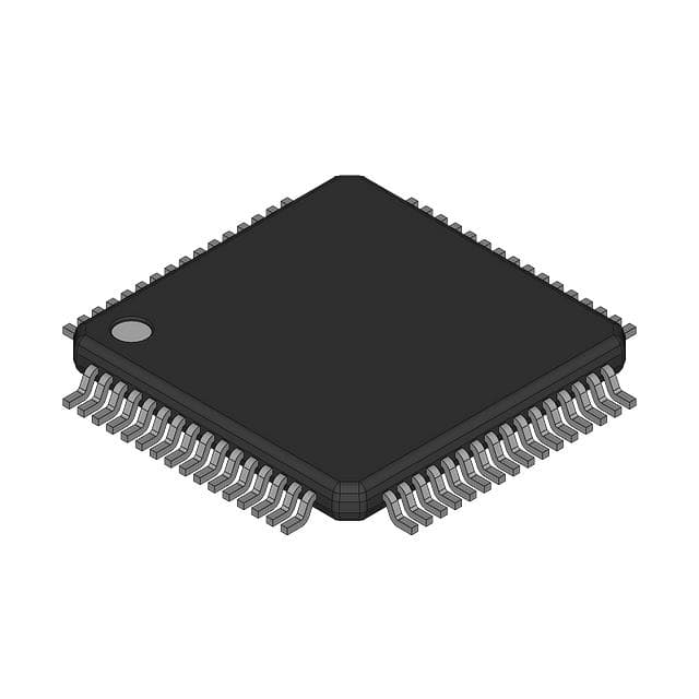
- Part No.:
- SN75FC1000PJD
- Manufacturer:
- Texas Instruments
- Category:
- Telecom
- Package:
- -
- Datasheet:
-
 SN75FC1000PJD.pdf
- Description:
- TELECOM CIRCUIT, PQFP64
- Quantity:
- Payment:

- Shipping:

Inventory:675
Please send an inquiry. Send us your inquiry, and we will respond immediately.
Product details
Overview
SN75FC1000PJD from Texas Instruments is a 1.0625 Gbps Fibre Channel transceiver IC compliant with ANSI X3T11 FC-PH-0 and supporting the 10-bit interface specification. It performs bidirectional SERDES for point-to-point data transmission over copper or optical media, operates at 3.3 V, features PECL differential I/O (DIN_RXP/DIN_RXN, DOUT_TXP/DOUT_TXN), and delivers 100 MBps bandwidth in storage area network (SAN) interconnects.
For engineers reviewing the SN75FC1000PJD datasheet, SN75FC1000PJD pinout, SN75FC1000PJD application, or SN75FC1000PJD equivalent, key selection considerations include its 64-pin HTQFP package with PowerPAD thermal enhancement, 53.125 MHz recovered byte clocks (RBC0/RBC1), 21 ns receive latency, 13 ns transmit latency, and support for 8b/10b encoded parallel-to-serial conversion with K28.5 comma alignment.
Technical Context
The SN75FC1000PJD integrates a PLL-based clock recovery circuit that locks to incoming 1.0625 Gbps serial data without external reference, or optionally to a 106.25 MHz REFCLK when LCKREFN is asserted. Its receiver extracts timing and deserializes data into aligned 10-bit words output on RD0–RD9 synchronized to two 180°-phase-shifted 53.125 MHz clocks (RBC0/RBC1).
The transmitter accepts 10-bit parallel data (TD0–TD9) on REFCLK rising edges, multiplies the clock by 10× to generate 1.0625 Gbaud NRZ serial output, and drives differential PECL signals with 1.2–2.2 Vpp swing into 50 Ω or 75 Ω loads. Internal loopback (LOOPEN) enables self-test by routing serialized output directly to the receiver path.
Key Specifications
| Parameter | Value and Actual Design Meaning |
|---|---|
| Data Rate | 1.0625 Gbps - supports full Fibre Channel 1x speed (100 MBps) with 8b/10b encoding overhead |
| Supply Voltage | 3.3 V ±3.5% - requires stable low-noise analog/digital rail separation (VCC_A, VCC_CMOS, VCC_TX, VCC_RX) |
| Differential I/O | PECL-compatible - 1.2–2.2 Vpp output swing into 50–75 Ω; 200 mV min differential input sensitivity |
| Latency | Transmit: 13 ns; Receive: 21 ns - fixed deterministic delay critical for timing-critical SAN link design |
| Recovery Clocks | RBC0 & RBC1 at 53.125 MHz - 180° out-of-phase, half-word-aligned outputs for byte-synchronous protocol interfacing |
| Operating Temp | 0°C to 70°C - commercial-grade temperature range suitable for controlled-environment server/storage chassis |
| Power Dissipation | 760–1085 mW (dynamic) - managed via thermal pad (PowerPAD) and segregated power domains |
Pinout & Package
SN75FC1000PJD uses a 64-pin HTQFP (PJD) package with exposed thermal pad (PowerPAD), JEDEC MS-026 compliant, 10 mm × 10 mm footprint, 1.20 mm max height, and 40°C/W junction-to-ambient thermal resistance.
| Pin/Terminal | Circuit Role | Design Meaning |
|---|---|---|
| DOUT_TXP / DOUT_TXN | Differential Transmit Output | NRZ serial data at 1.0625 Gbps; PECL levels; static when LOOPEN = high |
| DIN_RXP / DIN_RXN | Differential Receive Input | Accepts 1.0625 Gbps NRZ serial stream; 200 mV min differential input voltage |
| TD0–TD9 | Parallel Transmit Data Input | 10-bit 8b/10b encoded word latched on REFCLK rising edge |
| RD0–RD9 | Parallel Receive Data Output | Aligned 10-bit output referenced to RBC0/RBC1 rising edges; RD0 = LSB |
| RBC0 / RBC1 | Recovered Byte Clock Outputs | 53.125 MHz clocks, 180° out of phase; RBC1 aligns K28.5 character (byte 0) |
| REFCLK | Reference Clock Input | 106.25 MHz crystal-referenced clock for TX registration and RX PLL preset (when LCKREFN active) |
| LOOPEN | Loopback Enable Input | High = internal serial loopback; disables external I/O; enables functional self-test |
| SYNCEN / SYNC | Synchronization Control/Output | SYNCEN high enables K28.5 detection; SYNC pulses high for ½ REFCLK period on comma detection |
Key Features
| Feature | Design Value |
|---|---|
| ANSI X3T11 FC-PH-0 Compliance | Fully implements physical layer requirements for 1x Fibre Channel, including jitter tolerance (70% UI), lock time (500 µs), and K28.5 alignment |
| Integrated SERDES Architecture | Eliminates need for external serializer/deserializer; handles 10-bit parallel ↔ 1.0625 Gbps serial conversion with embedded clock recovery |
| Multi-Rail Power Isolation | Dedicated VCC_A, VCC_TX, VCC_RX, VCC_CMOS, VCC_TTL supplies minimize noise coupling between analog and digital sections |
| Thermal-Enhanced PowerPAD Package | PJD variant's exposed thermal pad reduces θJA to 40°C/W, enabling reliable operation at full dynamic power in compact SAN modules |
| Byte Alignment Without Protocol Overhead | RBC0/RBC1 clocks inherently align received bytes to 10-bit boundaries; eliminates need for additional framing logic in host controller |
Applications
| Fibre Channel Storage Interconnect | Server-to-Switch SAN Link |
|---|---|
Use Scenario: Point-to-point connection between Fibre Channel HBAs and fabric switches in enterprise storage arrays. IC Role / Device Role / Timing Role: Physical layer transceiver performing serialization/deserialization and clock recovery for 1.0625 Gbps FC-1 layer signaling. Use Value: Enables deterministic 100 MBps throughput with sub-25 ns end-to-end latency and built-in K28.5 word alignment for plug-and-play interoperability. | Use Scenario: Backplane or short-reach copper cable link between dual-processor servers and FC directors in clustered computing environments. IC Role / Device Role / Timing Role: High-speed bidirectional SERDES bridging parallel protocol logic to differential PECL physical interface. Use Value: Supports 3.3 V system integration with 5-V tolerant I/O, reducing level-shifting complexity while maintaining signal integrity up to 1.5 m trace length. |
| Optical Module Interface | Embedded SAN Controller PHY |
Use Scenario: Electrical interface to SFF-8472-compliant 1x Fibre Channel optical transceivers (e.g., 1310 nm LC duplex modules). IC Role / Device Role / Timing Role: PECL driver/receiver conditioning serial data for fiber-optic transmission; manages DC bias and common-mode voltage matching. Use Value: Delivers 1.2–2.2 Vpp differential swing compatible with industry-standard optical module inputs, eliminating external line drivers. | Use Scenario: Integrated PHY in ASIC-based Fibre Channel controllers for tape libraries or JBOD enclosures. IC Role / Device Role / Timing Role: Offloads SERDES, clock recovery, and word alignment from host processor; provides synchronous RD0–RD9 and RBC0/RBC1 outputs. Use Value: Reduces FPGA gate count and simplifies timing closure by delivering aligned parallel data with guaranteed setup/hold margins (≥3 ns). |
Equivalent & Alternatives
The following parts are listed as comparable options for similar Fibre Channel transceiver applications.
| Alternative Part | Technical Difference | Application Difference | Selection Advice |
|---|---|---|---|
| SN65LVDS100PJD | LVDS-based, 1.25 Gbps, no integrated clock recovery or 8b/10b encoder; requires external PLL and framing logic | Not FC-PH-0 compliant; suitable only for custom high-speed links without Fibre Channel protocol stack | Choose only if migrating away from Fibre Channel standards and accepting added system-level design complexity. |
| DS90CR285MTD | 28-bit LVDS serializer with separate deserializer; no native Fibre Channel features; max 1.188 Gbps aggregate | Lacks K28.5 detection, RBC clocks, and automatic word alignment; requires host-side framing | Select when building non-standard high-speed parallel-to-serial bridges where protocol independence outweighs FC compliance. |
Compared with SN65LVDS100PJD and DS90CR285MTD, the SN75FC1000PJD uniquely integrates full Fibre Channel PHY functionality-including clock recovery, 8b/10b handling, K28.5 alignment, and dual-byte clocks-enabling direct drop-in replacement in legacy FC-1 designs without modifying host interface logic or timing constraints.
Availability
SN75FC1000PJD is available at Aetrix Electronics and suitable for Fibre Channel storage interconnects, server-to-switch SAN links, optical module interfaces, and embedded SAN controller PHY implementations requiring stable component supply across extended product lifecycles.
Supply support for SN75FC1000PJD includes scheduled delivery planning, volume procurement assistance, BOM continuity management, traceable sourcing, and lifecycle availability coordination for OEM customers, industrial embedded developers, connected-device designers, and electronics production programs.
Manufacturer
Texas Instruments is a global semiconductor leader specializing in analog, embedded processing, and connectivity technologies, with decades of expertise in high-speed interface solutions.
The SN75FC1000PJD belongs to TI's Fibre Channel transceiver product line, designed specifically to enable cost-effective, standards-compliant 1x FC physical layer implementation in enterprise storage and server infrastructure.
FAQ
What is the primary function of the SN75FC1000PJD in a Fibre Channel system?
The SN75FC1000PJD serves as a complete physical layer transceiver, performing bidirectional serialization and deserialization of 10-bit parallel data at 1.0625 Gbps. It recovers clock from incoming serial streams, aligns data using K28.5 comma detection, and outputs synchronized parallel words on RD0–RD9 with RBC0/RBC1 clocks-enabling seamless integration with Fibre Channel protocol controllers without external SERDES or clock recovery ICs.
Does the SN75FC1000PJD require an external reference clock to operate?
The SN75FC1000PJD does not require an external reference clock for normal operation-it automatically locks to incoming 1.0625 Gbps serial data. However, REFCLK (106.25 MHz) is required when using LCKREFN for PLL preset or reset, and it clocks the TD0–TD9 parallel input. The device remains fully functional in standalone mode with only serial I/O and power applied.
How does the SN75FC1000PJD handle word alignment and synchronization?
The SN75FC1000PJD uses hardware-based K28.5 comma character detection to perform real-time 10-bit word alignment. When SYNCEN is high, it scans the serial stream for the 0011111010 pattern and adjusts RBC0/RBC1 timing to ensure RD0–RD9 outputs are byte-aligned. Misaligned commas trigger automatic 10-bit boundary shifts without data loss, and SYNC pulses indicate valid alignment events.
What are the thermal management requirements for the SN75FC1000PJD?
The SN75FC1000PJD in PJD package features a PowerPAD thermal pad that must be soldered to a large PCB copper pour for effective heat dissipation. With dynamic power up to 1085 mW, proper thermal design-including ≥4 cm² exposed copper connected to internal ground planes-is essential to maintain junction temperature below 125°C and achieve the rated 40°C/W θJA performance.
Is the SN75FC1000PJD still in production and supported by Texas Instruments?
No-the SN75FC1000PJD is marked OBSOLETE by Texas Instruments per official packaging information. While Aetrix Electronics maintains limited legacy inventory and offers lifecycle support, new designs should consider modern alternatives. TI no longer manufactures or warrants the SN75FC1000PJD, and technical documentation reflects 1998 revision status.
SN75FC1000PJD Specifications
- Product attributes
- Attribute value
- Manufacturer:
- Texas Instruments
- Series:
- *
- Package/Case:
- -
- Packaging:
- Bulk
- Product Status:
- Active
- Function:
- -
- Interface:
- -
- Number of Circuits:
- -
- Voltage - Supply:
- -
- Current - Supply:
- -
- Power (Watts):
- -
- Operating Temperature:
- -
- Grade:
- -
- Qualification:
- -
- Mounting Type:
- -
- Supplier Device Package:
- -
SN75FC1000PJD FAQ
1.How can I place an order for SN75FC1000PJD through Aetrix?
Please submit a Request for Quotation (RFQ) for SN75FC1000PJD on Aetrix. Our sales agent will provide a competitive quotation and guide you through the order confirmation once you accept the terms.
2.Are the price and stock information for SN75FC1000PJD reliable?
The price and inventory of SN75FC1000PJD are updated periodically and may fluctuate due to market conditions. Stock and pricing data are typically refreshed every 24 hours. Quotation validity for SN75FC1000PJD is usually 5 days.
3.What payment methods are accepted for SN75FC1000PJD?
We accept Wire Transfer, PayPal, Credit Card, Western Union, MoneyGram, and Escrow for SN75FC1000PJD transactions.
Note: Certain payment methods may incur a processing fee.
4.How is shipping managed for SN75FC1000PJD?
SN75FC1000PJD orders can be shipped via leading logistics carriers, including DHL, UPS, FedEx, TNT, or Registered Mail.
Once your SN75FC1000PJD order is processed, you will receive an email with the shipment details and tracking number.
Note: Tracking information may take up to 24 hours to appear. Express delivery typically takes 3–5 business days.
5.How can I obtain technical support or documentation for SN75FC1000PJD?
For technical support, including SN75FC1000PJD datasheets, pinout diagrams, or application guidance, please contact our engineering support team. They can provide detailed documentation and assistance for your SN75FC1000PJD requirements.
6.How does Aetrix verify that SN75FC1000PJD is sourced from the original manufacturer or authorized distributors?
All SN75FC1000PJD products on Aetrix are procured from qualified distributors and authorized channels. Our dedicated quality assurance team conducts strict verification, including traceability checks and, if necessary, third-party testing. This ensures that SN75FC1000PJD meets industry standards.
7.What is the process for return or replacement of SN75FC1000PJD?
All SN75FC1000PJD units undergo pre-shipment inspection (PSI). If there is an issue with SN75FC1000PJD, returns or replacements are accepted under the following conditions:
1.Quantity discrepancies, incorrect items, or visible external defects (such as breakage or corrosion), acknowledged by Aetrix.
2.The issue is reported within 90 days of delivery.
3.The SN75FC1000PJD part is unused and in its original packaging.
Return procedure for SN75FC1000PJD:
1.Submit a request within 90 days.
2.Obtain a Return Material Authorization (RMA) from Aetrix.
SN75FC1000PJD Tags

-
LMC567CMX/NOPB
Texas Instruments
-
LM567CMX/NOPB
Texas Instruments
-
LM567CM/NOPB
Texas Instruments

-
VSC8531XMW-02
Microchip Technology
-
VSC8531XMW-05
Microchip Technology

-
GPY115C0VI
MaxLinear, Inc.

-
SI32185-A-FMR
Skyworks Solutions Inc.

-
VSC8541XMV-05
Microchip Technology

-
SI32178-B-FM1R
Skyworks Solutions Inc.
-
GPY215C0VI
MaxLinear, Inc.

-
CPC7514ZTR
Littelfuse Inc.

-
VSC8502XML-03
Microchip Technology
Tech Hub

A practical engineering guide to 3.3V and 5V logic compatibility, input thresholds, resistor dividers, translator ICs, MOSFET level shifting, I2C pull-ups, timing limits and power-sequencing risks.

The 74HC595 uses push-pull logic outputs, while the TPIC6B595 uses 50 V open-drain DMOS sinks for higher-power loads. This guide compares timing, current limits, 3.3 V interfacing, load wiring, thermal…

The 74HC595 converts serial data into eight stable parallel outputs. This guide covers pin functions, shift and storage timing, OE and MR behavior, drive-current limits, cascading, voltage compatibilit…

A technical comparison of level-sensitive latches and edge-triggered flip-flops, covering timing windows, setup and hold limits, master–slave operation, time borrowing, race-through, HDL inference and…

A D latch stores one bit while Enable controls when data can pass. This reference covers gate-level operation, truth tables, transparency, setup and hold timing, LE versus OE, common ICs and practical …

An SR latch stores one bit through cross-coupled feedback. This engineering reference covers NOR and NAND implementations, truth tables, forbidden-state recovery, gated operation, switch debouncing, fa…

Latch circuits retain one bit through feedback. This technical reference covers SR and D latches, truth tables, transparency, timing limits, latch-versus-flip-flop behavior, applications and common log…

An engineering guide to LED driver operation, constant-current and constant-voltage outputs, linear and switching topologies, dimming, IC selection, calculations, replacement compatibility, and fault c…

Operational amplifier guide covering op amp basics, feedback, ideal vs real op amps, common configurations, buffer circuits, offset, bias current, gain-bandwidth, slew rate, rail-to-rail limits and sel…

Jumper cables guide covering safe connection order, red and black clamp placement, final ground connection, cable gauge, length, clamp quality, copper vs CCA cables, jump starter comparison and battery…


