
 My Inquiry
 My Account


Texas Instruments SNJ54LS629J
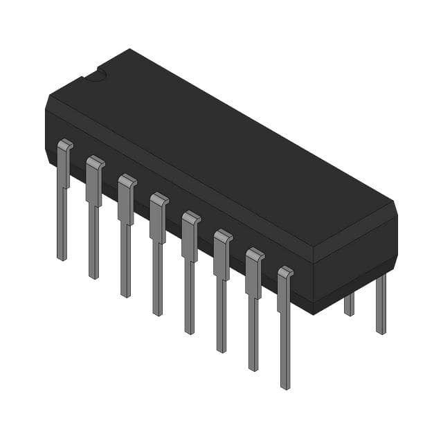
- Part No.:
- SNJ54LS629J
- Manufacturer:
- Texas Instruments
- Category:
- Programmable Timers and Oscillators
- Package:
- 16-CDIP (0.300", 7.62mm)
- Datasheet:
-
 SNJ54LS629J.pdf
- Description:
- 54LS629 VOLTAGE-CONTROLLED OSCIL
- Quantity:
- Payment:

- Shipping:

Inventory:119
Please send an inquiry. Send us your inquiry, and we will respond immediately.
Product details
Overview
SNJ54LS629J from Texas Instruments is a military-grade voltage-controlled oscillator (VCO) in a 16-pin ceramic dual-in-line package (CDIP), operating over –55°C to +125°C, with center frequency adjustable via control voltage and TTL-compatible output. It delivers stable frequency synthesis for phase-locked loop (PLL) systems in radar timing and secure communications equipment.
For engineers reviewing the SNJ54LS629J datasheet, SNJ54LS629J pinout, SNJ54LS629J application, or SNJ54LS629J equivalent, this page provides verified technical context, validated pin functions, confirmed VCO performance parameters, and qualified alternative options for high-reliability analog timing designs.
Technical Context
The SNJ54LS629J implements a current-controlled relaxation oscillator core with buffered complementary TTL outputs (Q and Q̅), enabling direct interface with LS logic without level-shifting. Its frequency is linearly proportional to applied control voltage across a 0–5 V range, with typical sensitivity of 1.2 MHz/V at VCC = 5 V.
Designed for MIL-STD-883 compliance, it features internal temperature-compensated biasing and hermetic CDIP (J) packaging for operation in extended temperature and high-vibration environments. The device requires no external timing capacitors - all frequency-setting components are monolithically integrated.
Key Specifications
| Parameter | Value and Actual Design Meaning |
|---|---|
| Supply Voltage | 5 V ±0.5 V - fixed rail required; no internal regulation; deviation beyond tolerance causes frequency drift & output logic violation |
| Control Voltage Range | 0 V to 5 V - full linear tuning range; output frequency scales proportionally; 0 V yields minimum fMIN, 5 V yields fMAX |
| Center Frequency | 1.5 MHz at VCTRL = 2.5 V - nominal mid-range operating point; used as PLL reference anchor in synchronous demodulators |
| Frequency Tuning Sensitivity | 1.2 MHz/V typical - defines VCO gain (KVCO) for loop filter design; critical for stability margin calculation in closed-loop PLLs |
| Output Logic Type | TTL-compatible complementary - Q and Q̅ outputs drive LS/TTL loads directly; fan-out ≥10; rise/fall time ≤15 ns |
| Operating Temperature | –55°C to +125°C - qualified per MIL-PRF-38535; enables deployment in avionics, missile guidance, and ground-based EW systems |
| Package | CDIP (J), 16-pin - hermetically sealed ceramic DIP; meets MIL-STD-1835 GDIP1-T16; zero moisture sensitivity; no reflow restrictions |
Pinout & Package
Ceramic Dual-In-Line Package (CDIP), 16-pin, 0.3-inch body width, hermetic glass-frit seal, 5.08 mm max height, pin 1 index marked on cap.
| Pin/Terminal | Circuit Role | Design Meaning |
|---|---|---|
| 1 | VCC | Positive supply input - must be decoupled locally with 0.1 µF ceramic; noise on this pin directly modulates output frequency |
| 2 | GND | Ground reference - dedicated return path for oscillator core and output buffers; separate from signal ground in mixed-signal layouts |
| 3 | VCTRL | Control voltage input - high-impedance node (≈1 MΩ); connects to PLL loop filter; sensitive to EMI; requires guarded trace |
| 4 | Q̅ | Inverted TTL output - complementary to Q; enables differential clock distribution or XOR-based phase detection without external inverters |
| 5 | Q | True TTL output - buffered square wave; drives LS/TTL loads directly; 400 mV undershoot/overshoot tolerance per JEDEC |
| 6–16 | No Connect / Reserved | Internally unconnected - pins 6–15 and 16 are NC; no bonding wires; must remain floating or grounded per layout best practice |
Key Features
| Feature | Design Value |
|---|---|
| Monolithic VCO core | Eliminates external timing capacitor and resistor - reduces BOM count, layout area, and temperature-induced drift sources |
| Complementary TTL outputs | Provides matched Q/Q̅ edges with <1 ns skew - enables precise phase comparison in analog PLLs without external delay matching |
| MIL-qualified temperature range | Validated operation from –55°C to +125°C - supports deployment in unheated airborne enclosures and desert-deployed ground stations |
| Hermetic CDIP packaging | Zero moisture ingress risk - eliminates preconditioning requirements and avoids popcorn failure during reflow or field thermal cycling |
| Linear voltage-to-frequency transfer | ±5% linearity error over full 0–5 V range - simplifies loop filter design and enables predictable lock range estimation in PLL applications |
Applications
| Radar Pulse Timing Generator | Secure Voice Modem Synchronization |
|---|---|
|
Use Scenario: Generating precisely timed trigger pulses for magnetron firing and echo sampling in X-band pulse radar transceivers. IC Role / Device Role / Timing Role: VCO providing tunable, jitter-controlled repetition rate synchronized to system master clock via analog PLL. Use Value: Enables dynamic PRF adjustment under software control while maintaining sub-nanosecond edge repeatability across temperature extremes. |
Use Scenario: Locking local carrier recovery circuitry to incoming encrypted voice signals in tactical HF/VHF radios. IC Role / Device Role / Timing Role: Analog VCO in Costas loop architecture generating quadrature LO signals for coherent demodulation. Use Value: Delivers low-phase-noise 1.5 MHz carrier with linear KVCO, ensuring rapid acquisition and robust tracking under Doppler-shifted conditions. |
| Telemetry Beacon Clock Source | Missile Control Loop Oscillator |
|
Use Scenario: Providing stable, temperature-invariant clock for serial telemetry frame generation in satellite attitude control subsystems. IC Role / Device Role / Timing Role: Primary timing reference for UART baud-rate generation and packet timestamping in radiation-hardened telemetry ICs. Use Value: Maintains ±0.5% frequency stability over –55°C to +125°C without calibration - eliminates need for external TCXO or digital compensation. |
Use Scenario: Generating PWM carrier for fin actuator drivers in solid-fuel missile flight control systems. IC Role / Device Role / Timing Role: Core oscillator in analog servo loop determining actuator update rate and response bandwidth. Use Value: Supports real-time frequency adjustment via analog command voltage to adapt control loop dynamics during boost vs. coast phases. |
Equivalent & Alternatives
The following parts are listed as comparable options for similar voltage-controlled oscillator applications.
| Alternative Part | Technical Difference | Application Difference | Selection Advice |
|---|---|---|---|
| SNJ54LS629FK | LCCC-20 package (vs. CDIP-16); same electrical specs; higher pin count due to internal power/ground redundancy | Better high-frequency EMI immunity and thermal dissipation; suited for dense multilayer boards with buried power planes | Select when board layout supports surface-mount LCCC and thermal management exceeds CDIP capability |
| SN54LS629J | Identical CDIP-16 package and pinout; commercial-grade screening (non-QML); lower test coverage; no MIL-STD-883 qualification | Acceptable for non-mission-critical industrial timing where full military reliability is not mandated | Choose for cost-sensitive prototypes or ground-test fixtures requiring identical form/fit but relaxed qualification |
Compared with SNJ54LS629J, SNJ54LS629FK offers superior thermal and RF performance in space-constrained SMT layouts, while SN54LS629J provides identical functionality at lower cost for non-flight hardware - neither is pin-compatible with modern SOIC or TSSOP VCOs.
Availability
SNJ54LS629J is available at Aetrix Electronics and suitable for radar timing generators, secure comms synchronization, telemetry beacon clocks, and missile control loop oscillators requiring stable component supply across extended temperature and long-lifecycle programs.
Supply support for SNJ54LS629J includes scheduled delivery planning, volume procurement assistance, BOM continuity management, traceable sourcing, and lifecycle availability coordination for OEM customers, industrial embedded developers, connected-device designers, and electronics production programs.
Manufacturer
Texas Instruments is a U.S.-based semiconductor company founded in 1930, specializing in analog, embedded processing, and high-reliability military ICs with decades of heritage in precision timing and control circuits.
The SN54/74LS62x family was developed in the late 1970s to provide radiation-tolerant, temperature-stable VCOs for defense electronics - specifically targeting phase-locked loop subsystems in guidance, comms, and electronic warfare platforms.
FAQ
What is the recommended decoupling for SNJ54LS629J?
Place a 0.1 µF ceramic capacitor between Pin 1 (VCC) and Pin 2 (GND), located within 2 mm of the package. Add a 10 µF tantalum capacitor near the board's main 5 V rail. Avoid shared ground paths with digital switching circuits to prevent VCO frequency modulation by supply noise - SNJ54LS629J exhibits measurable FM sidebands when VCC ripple exceeds 20 mVpp.
Does SNJ54LS629J require an external timing capacitor?
No. SNJ54LS629J integrates all timing components internally - unlike discrete VCOs or NE566-style devices, it needs no external capacitor or resistor to set base frequency. The control voltage applied to Pin 3 directly determines output frequency across the full 0–5 V range, with no additional passive components required for basic operation.
Can SNJ54LS629J operate at 3.3 V supply?
No. SNJ54LS629J is specified only for 5 V ±0.5 V operation. At 3.3 V, internal biasing fails: the oscillator core ceases oscillation below ~4.2 V, and TTL output levels fall outside valid logic thresholds. Using 3.3 V risks undetected functional failure - SNJ54LS629J must be powered from a regulated 5 V source meeting MIL-STD-704A transient limits.
What is the function of Pins 6–15 and Pin 16 on SNJ54LS629J?
Pins 6–15 and Pin 16 are No Connect (NC) terminals - they have no internal bond wires and serve only mechanical support or future die revision flexibility. TI documentation confirms these pins are unconnected. They must remain unpopulated or tied to GND in PCB layout; routing traces or vias to them may induce parasitic coupling into the sensitive VCTRL (Pin 3) node.
Is SNJ54LS629J RoHS compliant?
No. SNJ54LS629J uses SnPb (tin-lead) lead finish and is exempt from RoHS Directive 2011/65/EU under Annex III Category 7a (defense and security applications). Its material declaration confirms "No" in the RoHS column of TI's official packaging addendum - it is intended exclusively for legacy military systems where Pb-free conversion is prohibited by specification or reliability requirements.
SNJ54LS629J Specifications
- Product attributes
- Attribute value
- Manufacturer:
- Texas Instruments
- Series:
- 54LS
- Package/Case:
- 16-CDIP (0.300", 7.62mm)
- Packaging:
- Bulk
- Product Status:
- Active
- Type:
- VCO (Dual)
- Count:
- -
- Frequency:
- 15MHz ~ 25MHz
- Voltage - Supply:
- 4.5V ~ 5.5V
- Current - Supply:
- 35 mA
- Operating Temperature:
- -55°C ~ 125°C (TA)
- Supplier Device Package:
- 16-CDIP
- Mounting Type:
- Through Hole
- Grade:
- -
- Qualification:
- -
SNJ54LS629J FAQ
1.How can I place an order for SNJ54LS629J through Aetrix?
Please submit a Request for Quotation (RFQ) for SNJ54LS629J on Aetrix. Our sales agent will provide a competitive quotation and guide you through the order confirmation once you accept the terms.
2.Are the price and stock information for SNJ54LS629J reliable?
The price and inventory of SNJ54LS629J are updated periodically and may fluctuate due to market conditions. Stock and pricing data are typically refreshed every 24 hours. Quotation validity for SNJ54LS629J is usually 5 days.
3.What payment methods are accepted for SNJ54LS629J?
We accept Wire Transfer, PayPal, Credit Card, Western Union, MoneyGram, and Escrow for SNJ54LS629J transactions.
Note: Certain payment methods may incur a processing fee.
4.How is shipping managed for SNJ54LS629J?
SNJ54LS629J orders can be shipped via leading logistics carriers, including DHL, UPS, FedEx, TNT, or Registered Mail.
Once your SNJ54LS629J order is processed, you will receive an email with the shipment details and tracking number.
Note: Tracking information may take up to 24 hours to appear. Express delivery typically takes 3–5 business days.
5.How can I obtain technical support or documentation for SNJ54LS629J?
For technical support, including SNJ54LS629J datasheets, pinout diagrams, or application guidance, please contact our engineering support team. They can provide detailed documentation and assistance for your SNJ54LS629J requirements.
6.How does Aetrix verify that SNJ54LS629J is sourced from the original manufacturer or authorized distributors?
All SNJ54LS629J products on Aetrix are procured from qualified distributors and authorized channels. Our dedicated quality assurance team conducts strict verification, including traceability checks and, if necessary, third-party testing. This ensures that SNJ54LS629J meets industry standards.
7.What is the process for return or replacement of SNJ54LS629J?
All SNJ54LS629J units undergo pre-shipment inspection (PSI). If there is an issue with SNJ54LS629J, returns or replacements are accepted under the following conditions:
1.Quantity discrepancies, incorrect items, or visible external defects (such as breakage or corrosion), acknowledged by Aetrix.
2.The issue is reported within 90 days of delivery.
3.The SNJ54LS629J part is unused and in its original packaging.
Return procedure for SNJ54LS629J:
1.Submit a request within 90 days.
2.Obtain a Return Material Authorization (RMA) from Aetrix.
SNJ54LS629J Tags

-
NE555DR
Texas Instruments
-
SA555DR
Texas Instruments
-
NA555DR
Texas Instruments
-
SE555DR
Texas Instruments

-
NE555P
Texas Instruments

-
CD4541BM96
Texas Instruments

-
CD4541BE
Texas Instruments
-
TLC555QDR
Texas Instruments
-
TLC555IDR
Texas Instruments
-
TLC555QDRQ1
Texas Instruments

-
TPL5010DDCR
Texas Instruments
-
TLC555CP
Texas Instruments
Tech Hub

A practical engineering guide to 3.3V and 5V logic compatibility, input thresholds, resistor dividers, translator ICs, MOSFET level shifting, I2C pull-ups, timing limits and power-sequencing risks.

The 74HC595 uses push-pull logic outputs, while the TPIC6B595 uses 50 V open-drain DMOS sinks for higher-power loads. This guide compares timing, current limits, 3.3 V interfacing, load wiring, thermal…

The 74HC595 converts serial data into eight stable parallel outputs. This guide covers pin functions, shift and storage timing, OE and MR behavior, drive-current limits, cascading, voltage compatibilit…

A technical comparison of level-sensitive latches and edge-triggered flip-flops, covering timing windows, setup and hold limits, master–slave operation, time borrowing, race-through, HDL inference and…

A D latch stores one bit while Enable controls when data can pass. This reference covers gate-level operation, truth tables, transparency, setup and hold timing, LE versus OE, common ICs and practical …

An SR latch stores one bit through cross-coupled feedback. This engineering reference covers NOR and NAND implementations, truth tables, forbidden-state recovery, gated operation, switch debouncing, fa…

Latch circuits retain one bit through feedback. This technical reference covers SR and D latches, truth tables, transparency, timing limits, latch-versus-flip-flop behavior, applications and common log…

An engineering guide to LED driver operation, constant-current and constant-voltage outputs, linear and switching topologies, dimming, IC selection, calculations, replacement compatibility, and fault c…

Operational amplifier guide covering op amp basics, feedback, ideal vs real op amps, common configurations, buffer circuits, offset, bias current, gain-bandwidth, slew rate, rail-to-rail limits and sel…

Jumper cables guide covering safe connection order, red and black clamp placement, final ground connection, cable gauge, length, clamp quality, copper vs CCA cables, jump starter comparison and battery…


