
 My Inquiry
 My Account


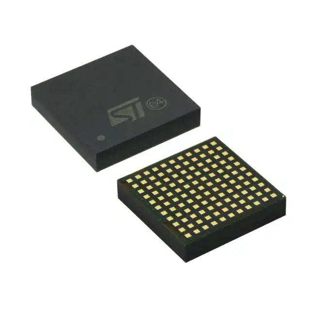
STMicroelectronics SPDC12L00010
- Part No.:
- SPDC12L00010
- Manufacturer:
- STMicroelectronics
- Category:
- DC DC Converters
- Package:
- 121-BLGA Module
- Datasheet:
-
 SPDC12L00010.pdf
- Description:
- DC DC CONVERTER 0.6-5V
- Quantity:
- Payment:

- Shipping:

Inventory:272
Please send an inquiry. Send us your inquiry, and we will respond immediately.
Product details
Overview
SPDC12L00010 from STMicroelectronics is a fully integrated 10 A step-down DC-DC converter module in LGA package, delivering 0.6–5 V output from 1.8–14 V input with 93% peak efficiency and 40 mVpp output ripple. It integrates controller, power FETs, inductor, and support components, enabling standalone point-of-load regulation in space-constrained server and telecom systems.
For engineers reviewing the SPDC12L00010 datasheet, SPDC12L00010 pinout, SPDC12L00010 application, or SPDC12L00010 equivalent, key selection criteria include its programmable soft-start, master/slave synchronization with 180° phase shift, selectable UVLO (5 V/12 V), pre-bias start-up, and Power Good with programmable delay - all critical for high-density distributed power architectures.
Technical Context
The SPDC12L00010 employs fixed-frequency voltage-mode control with internal 0.6 V reference (±1% tolerance) and synchronous rectification to achieve ultrafast transient response and stable regulation down to 0.6 V. Its integrated oscillator supports frequency adjustment via external resistor on OS pin and enables precise inter-module synchronization via SYNC pin.
Protection architecture includes latched or non-latched overvoltage protection (OVP), cycle-by-cycle overcurrent limiting (12 A trip), thermal shutdown at 120 °C case temperature, and programmable undervoltage lockout (UVLO) thresholds - all implemented without external components beyond PGDLY capacitor and SS_INL timing capacitor.
Key Specifications
| Parameter | Value and Actual Design Meaning |
|---|---|
| Output current | 10 A continuous; supports full load without heatsink or airflow in free-air conditions on 4-layer PCB |
| Input voltage range | 1.8 V to 14 V; dual-supply architecture allows separate VCC (4.5–14 V) and VIN rails |
| Output voltage range | 0.6 V to 5 V; programmed via FB pin with ±1% regulation accuracy over -40 °C to +85 °C |
| Peak efficiency | 93%; achieved at mid-load with 12 V input and 3.3 V/5 V output, minimizing thermal stress |
| Output ripple | 40 mVpp; measured at 12 V input, 10 A load, 2×330 μF output capacitance, 20 MHz BW |
| Switching frequency | 678–780 kHz; factory-trimmed, adjustable ±15% via OS pin resistor |
| Thermal shutdown | 120 °C at center of top case (T1); de-rates output current progressively above 75 °C ambient |
Pinout & Package
SPDC12L00010 uses a thermally enhanced 15 mm × 15 mm × 3 mm over-molded Land Grid Array (LGA) package with exposed thermal pad (PH bank) for bottom-side heat dissipation. The package is RoHS-compliant and designed for standard SMT reflow assembly, including back-side mounting.
| Pin/Terminal | Circuit Role | Design Meaning |
|---|---|---|
| VIN (Bank 1) | Primary power input | Accepts 1.8–14 V DC; must be decoupled per Section 5.18; supplies power stage only |
| VCC (L3) | Controller supply | 4.5–14 V rail for internal logic; can be tied to VIN if ≥4.5 V, otherwise requires separate supply |
| VOUT (Bank 3) | Regulated output | Delivers 0.6–5 V at up to 10 A; low-impedance path required per Section 5.19 |
| FB (L9) | Feedback sense | Inverting input of error amplifier; sets output voltage via external resistor divider referenced to 0.6 V |
| SS_INL (L11) | Soft-start/inhibit | Pull <0.5 V to disable; external capacitor sets soft-start ramp time (e.g., 3.3 nF ≈ 10 ms total) |
| PG (L4) | Power Good indicator | Open-collector output pulled low if VOUT deviates >±10% from target; 10 kΩ pull-up to VAUX |
| PGDLY (L5) | PG delay control | Capacitor-to-SGND sets rising-edge delay: PGdelay = 0.5 × CPGDLY (pF) in μs |
| SYNC (L6) | Frequency synchronization | Master/slave interface; enables 180° phase shift between modules when tied together |
| PRG (L7) | Multi-function configuration | Selects UVLO threshold (5 V/12 V bus), OVP latch mode, and post-soft-start sink capability |
| VAUX (J11) | Auxiliary 5 V supply | Internally regulated 4.5–5.5 V source for PRG/OS biasing; no external capacitor needed |
Key Features
| Feature | Design Value |
|---|---|
| Integrated power train | Combines controller, MOSFETs, shielded inductor, and compensation in single LGA module - eliminates 30+ discrete components |
| Pre-bias start-up | Enables safe turn-on into pre-charged output capacitors without reverse current or voltage overshoot |
| Programmable Power Good delay | Adjustable rising-edge delay (0–100 μs typical) avoids false PG assertion during output voltage ramp |
| Source/sink capability | Selectable post-soft-start current sink mode improves transient response under sudden load removal |
| Thermal de-rating table | Published derating curves per VOUT (0.7–5.0 V) and VIN (6–14 V) enable precise system-level thermal design without prototyping |
Applications
| Blade Servers | RAID Systems |
|---|---|
Use Scenario: Distributed 12 V–to–1.2 V conversion for multi-core CPU and memory VRMs in high-density chassis. IC Role / Device Role / Timing Role: Standalone point-of-load regulator replacing multi-phase controller + DrMOS solutions. Use Value: 15×15 mm footprint frees PCB area for signal routing; back-side mounting doubles board utilization. | Use Scenario: Independent 3.3 V/5 V rails for SAS/SATA drive controllers and cache buffers in storage enclosures. IC Role / Device Role / Timing Role: Primary DC-DC converter with programmable PG delay ensuring clean power sequencing across hot-swap bays. Use Value: Pre-bias start-up prevents data corruption during drive insertion; 93% efficiency reduces fan load in sealed enclosures. |
| Network Routers | Cellular Base Stations |
Use Scenario: 1.8 V and 2.5 V supplies for FPGA I/O banks and packet processing ASICs in line cards. IC Role / Device Role / Timing Role: Synchronized multi-module solution using SYNC pin to minimize input ripple and EMI in shared 12 V backplane. Use Value: 180° phase shift cuts input capacitor RMS current by ~30%, allowing smaller bulk capacitance. | Use Scenario: 0.7 V core supply for RF transceiver SoCs in remote radio units operating at -40 °C to +85 °C. IC Role / Device Role / Timing Role: High-accuracy, low-noise POL regulator with ±1% VREF stability and 40 mVpp ripple meeting 3GPP spectral mask requirements. Use Value: Ultrafast transient response maintains voltage within spec during burst-mode LTE transmission. |
Equivalent & Alternatives
The following parts are listed as comparable options for similar high-current integrated DC-DC converter applications.
| Alternative Part | Technical Difference | Application Difference | Selection Advice |
|---|---|---|---|
| TI TPS84A20 | 8 A max output, 2.5–6 V input, 0.6–3.6 V output; 7 mm × 7 mm QFN vs. 15 mm × 15 mm LGA | Lacks master/slave sync and pre-bias start-up; lower current rating limits use in 10 A FPGA cores | Preferred for compact, lower-current designs where board space is more constrained than thermal budget |
| Infineon IR3897 | 12 A max output, 4.5–18 V input, 0.6–3.3 V output; requires external inductor and compensation | Discrete power stage increases BOM count and layout sensitivity; no integrated soft-start capacitor | Chosen when design flexibility (e.g., custom inductors, higher Vin) outweighs integration benefits |
Compared with TPS84A20 and IR3897, SPDC12L00010 uniquely delivers 10 A in a self-contained LGA module with synchronization, pre-bias start-up, and programmable PG delay - making it optimal for thermally dense, high-reliability telecom and server applications where layout simplicity and robust sequencing are mandatory.
Availability
SPDC12L00010 is available at Aetrix Electronics and suitable for blade servers, RAID systems, and cellular base stations requiring stable component supply across extended temperature ranges and long production lifecycles.
Supply support for SPDC12L00010 includes scheduled delivery planning, volume procurement assistance, BOM continuity management, traceable sourcing, and lifecycle availability coordination for OEM customers, industrial embedded developers, connected-device designers, and electronics production programs.
Manufacturer
STMicroelectronics is a global semiconductor leader headquartered in Geneva, specializing in power management, microcontrollers, and analog ICs for industrial, automotive, and communications markets.
The SPDC series targets high-density point-of-load conversion, integrating complete DC-DC functionality into compact LGA modules to simplify power design in space- and thermal-constrained infrastructure equipment.
FAQ
What is the maximum allowable case temperature for continuous operation?
The SPDC12L00010 must not exceed 120 °C at the center of the top case (T1 point). Thermal de-rating tables in the datasheet specify reduced output current limits based on ambient temperature and input/output voltage combinations to maintain this limit on standard 4-layer FR4 PCBs.
Can SPDC12L00010 operate with an input voltage below 4.5 V?
Yes - the power stage (VIN) accepts 1.8 V minimum, but the controller (VCC) requires ≥4.5 V. Below 4.5 V on VIN, VCC must be supplied separately from a dedicated 4.5–14 V rail; tying VCC to VIN is only valid when VIN ≥4.5 V.
How is the Power Good delay calculated and what is its functional impact?
PG delay is set by a capacitor from PGDLY (L5) to SGND: PGdelay (μs) = 0.5 × CPGDLY (pF). This delay applies only to the rising edge of the PG signal, preventing false assertions during output voltage ramp-up while preserving immediate fault detection on falling edges.
Does SPDC12L00010 support output voltage tracking for multi-rail sequencing?
No - the device lacks dedicated tracking pins or analog control inputs for coordinated ramping with other supplies. Sequencing must be managed externally via inhibit (SS_INL) pin control or upstream power sequencers, as confirmed in Section 5.3 and Figure 5 of the datasheet.
SPDC12L00010 Specifications
- Product attributes
- Attribute value
- Manufacturer:
- STMicroelectronics
- Series:
- -
- Package/Case:
- 121-BLGA Module
- Packaging:
- Tray
- Product Status:
- Obsolete
- Type:
- Non-Isolated PoL Module
- Number of Outputs:
- 1
- Voltage - Input (Min):
- 1.8V
- Voltage - Input (Max):
- 14V
- Voltage - Output 1:
- 0.6 ~ 5V
- Voltage - Output 2:
- -
- Voltage - Output 3:
- -
- Voltage - Output 4:
- -
- Current - Output (Max):
- 10A
- Power (Watts):
- -
- Voltage - Isolation:
- -
- Applications:
- ITE (Commercial)
- Features:
- UVLO
- Operating Temperature:
- -40°C ~ 85°C
- Efficiency:
- 93%
- Grade:
- -
- Qualification:
- -
- Mounting Type:
- Surface Mount
- Supplier Device Package:
- -
- Control Features:
- -
- Approval Agency:
- -
- Standard Number:
- -
SPDC12L00010 FAQ
1.How can I place an order for SPDC12L00010 through Aetrix?
Please submit a Request for Quotation (RFQ) for SPDC12L00010 on Aetrix. Our sales agent will provide a competitive quotation and guide you through the order confirmation once you accept the terms.
2.Are the price and stock information for SPDC12L00010 reliable?
The price and inventory of SPDC12L00010 are updated periodically and may fluctuate due to market conditions. Stock and pricing data are typically refreshed every 24 hours. Quotation validity for SPDC12L00010 is usually 5 days.
3.What payment methods are accepted for SPDC12L00010?
We accept Wire Transfer, PayPal, Credit Card, Western Union, MoneyGram, and Escrow for SPDC12L00010 transactions.
Note: Certain payment methods may incur a processing fee.
4.How is shipping managed for SPDC12L00010?
SPDC12L00010 orders can be shipped via leading logistics carriers, including DHL, UPS, FedEx, TNT, or Registered Mail.
Once your SPDC12L00010 order is processed, you will receive an email with the shipment details and tracking number.
Note: Tracking information may take up to 24 hours to appear. Express delivery typically takes 3–5 business days.
5.How can I obtain technical support or documentation for SPDC12L00010?
For technical support, including SPDC12L00010 datasheets, pinout diagrams, or application guidance, please contact our engineering support team. They can provide detailed documentation and assistance for your SPDC12L00010 requirements.
6.How does Aetrix verify that SPDC12L00010 is sourced from the original manufacturer or authorized distributors?
All SPDC12L00010 products on Aetrix are procured from qualified distributors and authorized channels. Our dedicated quality assurance team conducts strict verification, including traceability checks and, if necessary, third-party testing. This ensures that SPDC12L00010 meets industry standards.
7.What is the process for return or replacement of SPDC12L00010?
All SPDC12L00010 units undergo pre-shipment inspection (PSI). If there is an issue with SPDC12L00010, returns or replacements are accepted under the following conditions:
1.Quantity discrepancies, incorrect items, or visible external defects (such as breakage or corrosion), acknowledged by Aetrix.
2.The issue is reported within 90 days of delivery.
3.The SPDC12L00010 part is unused and in its original packaging.
Return procedure for SPDC12L00010:
1.Submit a request within 90 days.
2.Obtain a Return Material Authorization (RMA) from Aetrix.
SPDC12L00010 Tags
-
1S4E_0505S1.5U
GAPTEC Electronic
-
TPS631000DRLR
Texas Instruments
-
XCL209F083DR
Torex Semiconductor Ltd
-
SC202AMLTRT
Semtech Corporation

-
NME1S0505SC
Murata Power Solutions Inc.
-
XCL101A501ER-G
Torex Semiconductor Ltd
-
RFM-0505S
Recom Power
-
TEA 1-0505E
Traco Power
-
MIC33153YHJ-TR
Microchip Technology
-
TEA 1-0505
Traco Power
-
TPSM863252RDXR
Texas Instruments
-
RFB-0505S
Recom Power
Tech Hub

A practical engineering and sourcing framework covering lifecycle verification, lifetime-buy calculations, replacement qualification, supplier checks and counterfeit-risk controls.

TTL and CMOS logic families differ in thresholds, loading, output drive, power and timing. This engineering guide compares 74HC and 74HCT, calculates noise margins and checks 3.3 V/5 V compatibility.

A practical engineering guide to 3.3V and 5V logic compatibility, input thresholds, resistor dividers, translator ICs, MOSFET level shifting, I2C pull-ups, timing limits and power-sequencing risks.

The 74HC595 uses push-pull logic outputs, while the TPIC6B595 uses 50 V open-drain DMOS sinks for higher-power loads. This guide compares timing, current limits, 3.3 V interfacing, load wiring, thermal…

The 74HC595 converts serial data into eight stable parallel outputs. This guide covers pin functions, shift and storage timing, OE and MR behavior, drive-current limits, cascading, voltage compatibilit…

A technical comparison of level-sensitive latches and edge-triggered flip-flops, covering timing windows, setup and hold limits, master–slave operation, time borrowing, race-through, HDL inference and…

A D latch stores one bit while Enable controls when data can pass. This reference covers gate-level operation, truth tables, transparency, setup and hold timing, LE versus OE, common ICs and practical …

An SR latch stores one bit through cross-coupled feedback. This engineering reference covers NOR and NAND implementations, truth tables, forbidden-state recovery, gated operation, switch debouncing, fa…

Latch circuits retain one bit through feedback. This technical reference covers SR and D latches, truth tables, transparency, timing limits, latch-versus-flip-flop behavior, applications and common log…

An engineering guide to LED driver operation, constant-current and constant-voltage outputs, linear and switching topologies, dimming, IC selection, calculations, replacement compatibility, and fault c…


