
 My Inquiry
 My Account


NXP Semiconductors SSL5511T/1J
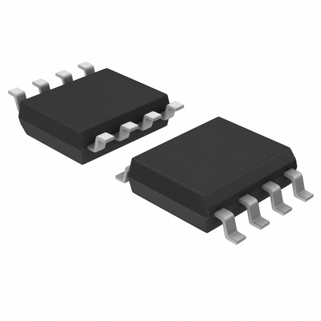
- Part No.:
- SSL5511T/1J
- Manufacturer:
- NXP Semiconductors
- Category:
- LED Drivers
- Package:
- 8-SOIC (0.154", 3.90mm Width)
- Datasheet:
-
 SSL5511T/1J.pdf
- Description:
- IC LED DRIVER OFFL ANALOG 8SO
- Quantity:
- Payment:

- Shipping:

Inventory:4,899
Please send an inquiry. Send us your inquiry, and we will respond immediately.
Product details
Overview
SSL5511T/1J from NXP Semiconductors is an offline dimmable LED controller IC for single-stage flyback, buck, and buck-boost topologies. It delivers ±4 % LED current accuracy, supports analog (IEC60929 Annex E) and digital dimming inputs, operates at 55–117 kHz switching frequencies, and integrates HV start-up JFET for direct mains-connected lighting applications such as GU10 and A19 smart lamps.
For engineers reviewing the SSL5511T/1J datasheet, SSL5511T/1J pinout, SSL5511T/1J application, or SSL5511T/1J equivalent, key selection considerations include dimming interface compatibility (analog vs. digital), selectable LTHD/low-ripple modes, primary-side sensing accuracy, integrated protections (OCP, OTP, OVP, UVLO), and SO8 package constraints for compact LED driver PCBs.
Technical Context
The SSL5511T/1J implements discontinuous conduction mode (DCM) peak-current control with valley-switching to minimize capacitive losses. It uses RMAINS pin sensing for mains synchronization and THD shaping, and supports three operational modes-LTHD (PF > 0.9), eco-LTHD (PF ≈ 0.75), and low-ripple (PF < 0.7)-selected via external resistors on PWRDRV and ISNS pins.
Dimming is handled through automatic detection of analog voltage (0.1–1.2 V) or digital signal (0.1–10 kHz, 0.3–1.75 V thresholds) on the DIM pin, with continuous analog regulation of LED current in both modes. Protection logic includes latched OVP, auto-restart OTP, and mains-loss detection with 50–60 ms delay.
Key Specifications
| Parameter | Value and Actual Design Meaning |
|---|---|
| VCC Range | 8.8 V to 32 V - powers IC after startup; internal HV JFET enables direct high-voltage start-up from DRAIN pin |
| fsw Range | 55–117 kHz - dual-frequency selection (LF/HF) balances efficiency vs. size; 50/60 Hz mains-synchronized |
| LED Current Accuracy | ±4 % - maintained across line, load, and component variations using primary-side sensing and adaptive regulation |
| Dimming Input Support | Analog (0.1–1.2 V) or digital (0.1–10 kHz) - auto-detected at startup; enables IEC60929-compliant remote control and PWM-based smart lamp interfaces |
| Protection Features | UVLO, OCP, OTP, OVP (latched), OSP, brownout, mains sync loss, LEB - ensures robust operation in unregulated AC environments without secondary feedback |
| Max DRAIN Voltage | 700 V - withstands surge transients in 230 V AC mains applications; rated for 25,000-hour lifetime at peak stress |
| Package | SO8 (SOT96-1) - 3.9 mm body width; optimized for thermally constrained LED lamp form factors including PAR, GU10, and A19 |
Pinout & Package
SSL5511T/1J is housed in an 8-pin SO8 plastic small outline package (SOT96-1), with 3.9 mm body width and standard JEDEC footprint. Thermal resistance is 159 K/W (free air, 2-layer 2 cm × 3 cm PCB).
| Pin/Terminal | Circuit Role | Design Meaning |
|---|---|---|
| RMAINS (1) | Mains detection input | Senses rectified AC waveform for synchronization, THD shaping, and low-ripple mode timing; triggers mains-loss protection if signal absent |
| VCC (2) | IC supply input/output | Charged by internal HV JFET at startup; supplies internal circuitry; OVP/UVLO thresholds (28–32 V / 8.8–9.8 V) define safe operating window |
| DIM (3) | Dim-level and on/off control | Accepts analog voltage or digital signal; auto-detects type; sets target LED current level; enters standby if input remains low >10 ms |
| TST (4) | IC test pin | Must be connected to GND in all applications; not used in normal operation |
| ISNS (5) | Peak current sense input | Monitors voltage across external sense resistor; threshold varies by mode (0.35 V low-ripple, 0.78 V eco-LTHD, 1.24 V high-threshold) |
| PWRDRV (6) | External MOSFET gate driver | Drives gate with 360 mA source / 900 mA sink capability; output clamped to ≤10.7 V; controls switch turn-on timing |
| GND (7) | Ground reference | Common return for internal circuitry, sense paths, and driver output; requires low-impedance PCB connection |
| DRAIN (8) | External MOSFET drain sense | Provides energy for VCC charging at startup; detects demagnetization and valley points for zero-voltage switching |
Key Features
| Feature | Design Value |
|---|---|
| Primary-side constant current regulation | Eliminates optocoupler and secondary-side feedback components, reducing BOM count and improving reliability in isolated LED drivers |
| Selectably optimized power factor or ripple performance | External resistor configuration enables trade-off between THD (<5% in LTHD mode) and LED current ripple (<5% in low-ripple mode) without topology change |
| Integrated HV start-up JFET | Enables direct connection to rectified mains; removes need for external start-up resistor network and associated power loss |
| Valley-switching with leading-edge blanking | Reduces switching losses and EMI; LEB (600 ns) prevents false overcurrent triggering during MOSFET turn-on spikes |
| Auto-detecting dimming interface | Supports legacy analog wall dimmers and modern digital controllers (e.g., DALI-2, proprietary RF) on same pin without external configuration |
Applications
| Smart Residential Lamps | Remote-Controlled Downlights |
|---|---|
Use Scenario: GU10 or A19 LED retrofit lamps controlled via RF remote or smartphone app with smooth dimming down to 0.8 % of full scale. IC Role / Device Role: Offline LED controller managing primary-side current regulation, dimming translation, and valley-switched MOSFET drive in compact single-stage flyback topology. Use Value: Enables certified IEC60929 analog dimming and digital PWM dimming in same hardware; ±4 % current accuracy ensures consistent lumen output across units and temperature. | Use Scenario: Mains-powered recessed downlight with wall-mounted touch dimmer and built-in indicator LED during standby. IC Role / Device Role: Dimmable LED driver IC providing low-standby-current operation (0.1 mA), mains synchronization, and brownout protection for stable dimming at 100–230 V AC. Use Value: Integrated HV start-up and VCC current budgeting support indicator LED functionality without auxiliary winding or extra regulators. |
| Compact PAR30/38 Luminaires | Universal-Voltage Smart Bulbs |
Use Scenario: High-lumen PAR30 spotlight (25 W) with thermal derating and overvoltage protection for commercial retail lighting. IC Role / Device Role: Primary-side regulated LED controller implementing OTP (175 °C trip), latched OVP, and output short protection without secondary sensing. Use Value: Eliminates need for discrete thermal cutoffs or Zener-based OVP; junction temperature monitoring ensures lamp lifetime matches LED source (≥25,000 hrs). | Use Scenario: Dual-voltage (100–240 V AC) smart bulb supporting voice-controlled dimming and scheduled on/off via Wi-Fi gateway. IC Role / Device Role: Dimmable offline controller enabling universal input operation via RMAINS-based mains detection and adaptive frequency scaling (55–117 kHz). Use Value: Single bill-of-material supports global markets; eco-LTHD mode achieves PF > 0.75 and THD < 20 % at 230 V AC while maintaining compact PCB area. |
Equivalent & Alternatives
The following parts are listed as comparable options for similar LED controller applications.
| Alternative Part | Technical Difference | Application Difference | Selection Advice |
|---|---|---|---|
| ON Semiconductor NCL30001DR2G | Fixed 65 kHz frequency; no digital dimming support; requires external HV start-up resistor | Limited to analog-dimming-only designs; lacks auto-detecting DIM interface and valley-switching | Choose for cost-sensitive, non-smart lamp applications where digital control and ultra-low ripple are unnecessary |
| Infineon ICE2QS03G | Quasi-resonant flyback controller; no integrated DIM pin logic; requires external dimming translator circuit | Needs additional components for IEC60929 compliance; no native digital signal handling or standby current optimization | Prefer when leveraging Infineon's QR ecosystem and secondary-side feedback is acceptable for tighter regulation |
Compared with NCL30001DR2G and ICE2QS03G, the SSL5511T/1J uniquely integrates analog/digital dimming auto-detection, valley-switching, and HV start-up in SO8 - reducing component count by ≥30 % and enabling direct replacement in smart lamp designs requiring <10 ms standby response and ±4 % current accuracy.
Availability
SSL5511T/1J is available at Aetrix Electronics and suitable for smart residential lamps, remote-controlled downlights, compact PAR luminaires, universal-voltage bulbs, and commercial LED retrofit applications requiring stable component supply and long-term lifecycle support.
Supply support for SSL5511T/1J includes scheduled delivery planning, volume procurement assistance, BOM continuity management, traceable sourcing, and lifecycle availability coordination for OEM customers, industrial embedded developers, connected-device designers, and electronics production programs.
Manufacturer
NXP Semiconductors is a Dutch semiconductor company specializing in secure connectivity solutions for automotive, industrial, and IoT applications, with leadership in energy-efficient power management ICs.
The SSL5511T/1J belongs to NXP's GreenChip LED controller product line, designed specifically for high-efficiency, dimmable, single-stage offline LED drivers targeting compact, mains-connected smart lighting with minimal BOM and certification-ready performance.
FAQ
What dimming protocols does the SSL5511T/1J natively support?
The SSL5511T/1J natively supports analog dimming per IEC60929 Annex E (0.1–1.2 V input) and digital PWM dimming (0.1–10 kHz, 0.3–1.75 V logic levels) on the same DIM pin. It automatically detects the input type at startup and applies appropriate translation to LED current. The SSL5511T/1J does not implement DALI, 0–10 V, or phase-cut protocols internally - those require external translators.
How does the SSL5511T/1J achieve ±4 % LED current accuracy without secondary feedback?
The SSL5511T/1J achieves ±4 % LED current accuracy using primary-side sensing with adaptive regulation: it monitors ISNS voltage, correlates it with DRAIN ringing valley timing and RMAINS-synchronized mains phase, and dynamically adjusts switching frequency and peak current threshold. This eliminates optocoupler drift and transformer variation errors. The SSL5511T/1J maintains this accuracy across 100–240 V AC input, –40 to +125 °C ambient, and component tolerances.
Can the SSL5511T/1J be used in buck topology with universal AC input?
Yes, the SSL5511T/1J supports buck topology with universal AC input (100–240 V AC) when configured with RTF = 56 kΩ on PWRDRV and RCTL = 5.6 kΩ on ISNS for LTHD mode. However, buck operation requires a high-voltage-rated LED string (>350 V) and careful layout to manage high-side switching noise. The SSL5511T/1J datasheet confirms buck operation in Section 8.2.1 and Figure 3, with Vi(DRAIN) rating up to 700 V ensuring safe operation.
What protection features are latched versus auto-restarting in the SSL5511T/1J?
Only Output open OverVoltage Protection (OVP) is latched in the SSL5511T/1J - it requires power-cycle recovery. All other protections - UVLO, OCP, OTP, OSP, brownout, mains sync loss, and LEB - are auto-restarting. After fault clearance, the SSL5511T/1J resumes operation within 1–9 seconds depending on protection type (e.g., 1 s for UVLO, 9 s for OSP), as defined in Sections 8.3.1–8.3.8 of the SSL5511T/1J datasheet.
Is the SSL5511T/1J compatible with wall switches that have indicator LEDs?
Yes, the SSL5511T/1J is explicitly designed for compatibility with wall switches containing indicator LEDs. Its VCC pin draws a controlled standby current (0.1–1.5 mA depending on VCC level) during limited voltage windows, preventing false triggering or flicker. This behavior is documented in Section 8.1.2 and Table 7 (ICC specifications), making the SSL5511T/1J suitable for retrofit lamps using standard household dimmers with neon or LED indicators.
SSL5511T/1J Specifications
- Product attributes
- Attribute value
- Manufacturer:
- NXP Semiconductors
- Series:
- GreenChip™
- Package/Case:
- 8-SOIC (0.154", 3.90mm Width)
- Packaging:
- Tape & Reel (TR)
- Product Status:
- Discontinued at Digi-Key
- Type:
- AC DC Offline Switcher
- Topology:
- Flyback, SEPIC, Step-Down (Buck), Step-Up (Boost)
- Internal Switch(s):
- No
- Number of Outputs:
- 1
- Voltage - Supply (Min):
- 8.8V
- Voltage - Supply (Max):
- 32V
- Voltage - Output:
- -
- Current - Output / Channel:
- -
- Frequency:
- -
- Dimming:
- Analog
- Applications:
- Lighting
- Operating Temperature:
- -40°C ~ 125°C (TA)
- Grade:
- -
- Qualification:
- -
- Mounting Type:
- Surface Mount
- Supplier Device Package:
- 8-SO
SSL5511T/1J FAQ
1.How can I place an order for SSL5511T/1J through Aetrix?
Please submit a Request for Quotation (RFQ) for SSL5511T/1J on Aetrix. Our sales agent will provide a competitive quotation and guide you through the order confirmation once you accept the terms.
2.Are the price and stock information for SSL5511T/1J reliable?
The price and inventory of SSL5511T/1J are updated periodically and may fluctuate due to market conditions. Stock and pricing data are typically refreshed every 24 hours. Quotation validity for SSL5511T/1J is usually 5 days.
3.What payment methods are accepted for SSL5511T/1J?
We accept Wire Transfer, PayPal, Credit Card, Western Union, MoneyGram, and Escrow for SSL5511T/1J transactions.
Note: Certain payment methods may incur a processing fee.
4.How is shipping managed for SSL5511T/1J?
SSL5511T/1J orders can be shipped via leading logistics carriers, including DHL, UPS, FedEx, TNT, or Registered Mail.
Once your SSL5511T/1J order is processed, you will receive an email with the shipment details and tracking number.
Note: Tracking information may take up to 24 hours to appear. Express delivery typically takes 3–5 business days.
5.How can I obtain technical support or documentation for SSL5511T/1J?
For technical support, including SSL5511T/1J datasheets, pinout diagrams, or application guidance, please contact our engineering support team. They can provide detailed documentation and assistance for your SSL5511T/1J requirements.
6.How does Aetrix verify that SSL5511T/1J is sourced from the original manufacturer or authorized distributors?
All SSL5511T/1J products on Aetrix are procured from qualified distributors and authorized channels. Our dedicated quality assurance team conducts strict verification, including traceability checks and, if necessary, third-party testing. This ensures that SSL5511T/1J meets industry standards.
7.What is the process for return or replacement of SSL5511T/1J?
All SSL5511T/1J units undergo pre-shipment inspection (PSI). If there is an issue with SSL5511T/1J, returns or replacements are accepted under the following conditions:
1.Quantity discrepancies, incorrect items, or visible external defects (such as breakage or corrosion), acknowledged by Aetrix.
2.The issue is reported within 90 days of delivery.
3.The SSL5511T/1J part is unused and in its original packaging.
Return procedure for SSL5511T/1J:
1.Submit a request within 90 days.
2.Obtain a Return Material Authorization (RMA) from Aetrix.
SSL5511T/1J Tags

-
BCR402RE6327HTSA1
Infineon Technologies

-
BCR430UXTSA2
Infineon Technologies

-
BCR420UE6433HTMA1
Infineon Technologies
-
BCR420UE6327HTSA1
Infineon Technologies
-
BCR421UE6327HTSA1
Infineon Technologies

-
LYT1604D-TL
Power Integrations

-
HV9910CLG-G
Microchip Technology

-
CL2N8-G
Microchip Technology

-
BCR420UW6-7
Diodes Incorporated
-
BCR421UW6-7
Diodes Incorporated

-
BCR420UFD-7
Diodes Incorporated
-
BCR421UFD-7
Diodes Incorporated
Tech Hub

A practical engineering guide to 3.3V and 5V logic compatibility, input thresholds, resistor dividers, translator ICs, MOSFET level shifting, I2C pull-ups, timing limits and power-sequencing risks.

The 74HC595 uses push-pull logic outputs, while the TPIC6B595 uses 50 V open-drain DMOS sinks for higher-power loads. This guide compares timing, current limits, 3.3 V interfacing, load wiring, thermal…

The 74HC595 converts serial data into eight stable parallel outputs. This guide covers pin functions, shift and storage timing, OE and MR behavior, drive-current limits, cascading, voltage compatibilit…

A technical comparison of level-sensitive latches and edge-triggered flip-flops, covering timing windows, setup and hold limits, master–slave operation, time borrowing, race-through, HDL inference and…

A D latch stores one bit while Enable controls when data can pass. This reference covers gate-level operation, truth tables, transparency, setup and hold timing, LE versus OE, common ICs and practical …

An SR latch stores one bit through cross-coupled feedback. This engineering reference covers NOR and NAND implementations, truth tables, forbidden-state recovery, gated operation, switch debouncing, fa…

Latch circuits retain one bit through feedback. This technical reference covers SR and D latches, truth tables, transparency, timing limits, latch-versus-flip-flop behavior, applications and common log…

An engineering guide to LED driver operation, constant-current and constant-voltage outputs, linear and switching topologies, dimming, IC selection, calculations, replacement compatibility, and fault c…

Operational amplifier guide covering op amp basics, feedback, ideal vs real op amps, common configurations, buffer circuits, offset, bias current, gain-bandwidth, slew rate, rail-to-rail limits and sel…

Jumper cables guide covering safe connection order, red and black clamp placement, final ground connection, cable gauge, length, clamp quality, copper vs CCA cables, jump starter comparison and battery…


