
 My Inquiry
 My Account


NXP Semiconductors SSTUG32868ET/G,518
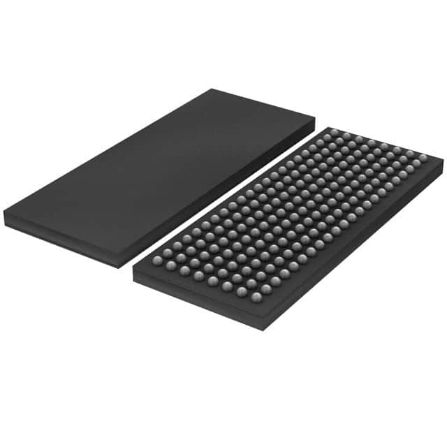
- Part No.:
- SSTUG32868ET/G,518
- Manufacturer:
- NXP Semiconductors
- Category:
- Specialty Logic
- Package:
- 176-TFBGA
- Datasheet:
-
 SSTUG32868ET/G,518.pdf
- Description:
- IC BUFFER 1.8V 25BIT 176-LFBGA
- Quantity:
- Payment:

- Shipping:

Inventory:4,860
Please send an inquiry. Send us your inquiry, and we will respond immediately.
Product details
Overview
SSTUG32868ET/G from NXP Semiconductors is a 1.8 V, 28-bit, 1:2 configurable registered buffer with integrated parity checking, designed specifically for DDR2-1G RDIMM applications in 2R×4 high-density memory modules. It integrates dual JEDEC-standard register functionality into one TFBGA176 package, supports up to 450 MHz clock frequency, delivers controlled multi-impedance output drivers, and features open-drain QERR error indication (active LOW).
For engineers reviewing the SSTUG32868ET/G datasheet, SSTUG32868ET/G pinout, SSTUG32868ET/G application, or SSTUG32868ET/G equivalent, key selection criteria include its 28-bit 1:2 register architecture, SSTL_18 data input compatibility, differential CK/CK clock interface, permanent high-output-drive configuration, and dual chip-select gating for low-power DIMM operation.
Technical Context
The SSTUG32868ET/G implements a dual-register architecture (Register A and Register B) selected via LVCMOS C input, enabling two distinct 22-bit data routing configurations per register bank. Its parity engine accepts PAR_IN one clock cycle after data, compares against D1–D28 inputs (subset dependent on C state), and asserts QERR two cycles later-latched LOW for ≥2 clocks or until RESET.
It uses differential CK/CK inputs with 600 mV minimum VID and 0.675–1.125 V common-mode range, supports SSTL_18 data inputs (VIH(AC) = Vref + 0.25 V), and provides gated outputs (QnA/QnB) disabled when CSGEN, DCS0, and DCS1 are HIGH-enabling low-power standby without board-level changes.
Key Specifications
| Parameter | Value and Actual Design Meaning |
|---|---|
| Supply Voltage | 1.7 V to 2.0 V nominal; enables stable operation across DDR2 VDD tolerance band with 1.8 V typical. |
| Max Clock Frequency | 450 MHz; supports DDR2-900 data rates (450 MT/s per pin) in high-density RDIMMs. |
| Propagation Delay | 1.0–1.4 ns (tPDM); ensures tight timing margin for high-speed DDR2 command/address/data re-driving. |
| Output Impedance | 7 Ω instantaneous / 53 Ω steady-state; optimizes signal integrity on unterminated DIMM stubs. |
| Parity Coverage | 22 data bits (D1–D12, D17–D28 plus D1/D7/D9–D12 depending on C state); even-parity validation with QERR active-LOW latching. |
| Operating Temperature | 0 °C to +70 °C; qualified for commercial-grade RDIMM deployment in server and workstation memory subsystems. |
| Package | TFBGA176, 6 mm × 15 mm, 0.65 mm ball pitch; enables high I/O density and escape routing in constrained DIMM layouts. |
Pinout & Package
Package: 176-ball thin fine-pitch ball grid array (TFBGA), 8 × 22 grid, 0.65 mm pitch, 6 mm × 15 mm body size, 0.7 mm height.
| Pin/Terminal | Circuit Role | Design Meaning |
|---|---|---|
| D1–D28 | Data inputs | SSTL_18 inputs clocked on CK/CK crossing; subset active based on C input (Register A/B mode). |
| Q1A–Q28A, Q1B–Q28B | Data outputs | 1.8 V CMOS outputs; QnA/QnB driven only when corresponding DCSn is LOW (gated by CSGEN/DCS0/DCS1). |
| CK / CK | Differential clock inputs | Accepts 600 mV min differential swing; common-mode range 0.675–1.125 V; defines all register timing edges. |
| PAR_IN | Parity input | SSTL_18 input arriving one clock cycle after associated data; used for even-parity comparison across 22 bits. |
| QERR | Open-drain error output | Active-LOW; latched LOW for ≥2 clock cycles on parity error; remains asserted through Low-Power Mode if error occurs pre-entry. |
| C | Configuration control | LVCMOS input selecting Register A (C = LOW) or Register B (C = HIGH); must be hard-wired, not toggled in operation. |
| CSGEN, DCS0–DCS3 | Chip select controls | LVCMOS/SSTL_18 inputs enabling/disabling output drive; CSGEN gates D-input latching; DCSn gate Q-output state changes. |
| RESET | Asynchronous reset | LVCMOS input forcing all registers to zero and Qn outputs LOW; disables differential receivers when LOW. |
| VREF | Reference voltage input | 0.9 V nominal (50% of VDD); internally tied between A5/AB5; only one pin requires external connection. |
| VDD / GND | Power / ground | 36 dedicated VDD balls and 40 GND balls distributed across package for low-noise, low-inductance supply delivery. |
Key Features
| Feature | Design Value |
|---|---|
| Integrated dual-register function | Replaces two discrete JEDEC-standard DDR2 registers (e.g., SSTUA32864 or SSTUA32866) in single TFBGA176 package-reducing PCB area and simplifying routing. |
| Configurable 1:2 register mapping | Pinout and data channel assignment dynamically selected via C input (Register A or B), supporting flexible DIMM layout and signal assignment. |
| Hardware parity checking | Real-time even-parity validation across 22 DIMM-independent data bits with latched QERR output-enabling system-level error detection without host CPU intervention. |
| Permanent high-output-drive strength | Optimized for heavy net loading in high-density RDIMMs; eliminates need for external termination or drive boosters. |
| Four independent chip-select inputs | DCS0–DCS3 allow granular gating of output states and QERR; reduces dynamic power by preventing unnecessary output transitions during idle cycles. |
| Controlled multi-impedance outputs | 7 Ω instantaneous / 53 Ω steady-state impedance ensures clean edge rates (1–4 V/ns) and minimal reflections on unterminated DIMM stubs. |
Applications
| Server Memory Modules | Workstation RDIMMs |
|---|---|
Use Scenario: High-density 2R×4 DDR2-900 RDIMMs deployed in dual-socket Xeon-based servers requiring ECC-capable memory subsystems. IC Role / Device Role / Timing Role: Registered buffer re-drives address/command/data signals from memory controller to two ranks of DDR2 SDRAM; provides clock deskew and parity validation. Use Value: Enables 400–800 MT/s operation with deterministic timing, reduces signal integrity risk on long DIMM traces, and adds hardware-level parity error flagging for RAS firmware. | Use Scenario: Dual-rank DDR2 RDIMMs used in high-end engineering workstations running memory-intensive CAD/CAE applications. IC Role / Device Role / Timing Role: Configurable 1:2 register buffers data paths for rank selection while maintaining strict tAC/tSU/tH compliance at 450 MHz. Use Value: Supports flexible DIMM population schemes (e.g., 2×4 vs. 1×8) via C-pin configuration; high-drive outputs maintain signal fidelity across varied trace lengths and loads. |
| Enterprise Storage Controllers | Communications Baseband Cards |
Use Scenario: DDR2 memory subsystems in RAID controllers and storage accelerators where reliability and thermal stability are critical. IC Role / Device Role / Timing Role: Parity-enabled registered buffer ensures data path integrity between controller ASIC and DDR2 memory banks; QERR feeds fault-monitoring logic. Use Value: Detects bit errors introduced during signal propagation-not just DRAM cell errors-improving end-to-end data path coverage beyond standard ECC. | Use Scenario: DDR2-based baseband processing cards in wireless infrastructure equipment operating in thermally constrained environments. IC Role / Device Role / Timing Role: Low-power active register with DCS-gated outputs minimizes dynamic power during bursty traffic patterns while maintaining 450 MHz throughput. Use Value: Four chip-select inputs enable precise power gating per functional block; CSGEN+DCS0/DCS1 combination cuts register output switching by >90% during idle periods. |
Equivalent & Alternatives
The following parts are listed as comparable options for similar DDR2 registered buffer applications.
| Alternative Part | Technical Difference | Application Difference | Selection Advice |
|---|---|---|---|
| IDT72V2225L15PF | 16-bit, non-parity, 3.3 V operation; no differential clock support; TQFP-100 package. | Lacks parity checking, operates at higher voltage, and does not support DDR2 SSTL_18 signaling or 450 MHz clocking. | Select only for legacy 3.3 V DDR1 or non-parity DDR2 designs where pin count and voltage compatibility permit. |
| ON Semiconductor NB3N551DR2G | 8-bit, no register function; clock buffer only; no data path or parity capability; SOIC-8 package. | Provides clock distribution only-no data re-driving, no address/command buffering, and no parity logic. | Use solely for clock fanout in systems where DDR2 register functionality is implemented elsewhere. |
Compared with IDT72V2225L15PF and NB3N551DR2G, the SSTUG32868ET/G uniquely delivers 28-bit 1:2 registered buffering with hardware parity, SSTL_18 compatibility, differential clock interface, and 450 MHz performance in a space-efficient TFBGA176-making it irreplaceable for modern DDR2-900 RDIMM designs requiring reliability and density.
Availability
SSTUG32868ET/G is available at Aetrix Electronics and suitable for server memory modules, enterprise storage controllers, and communications baseband cards requiring stable component supply, full lifecycle support, and guaranteed traceability.
Supply support for SSTUG32868ET/G includes scheduled delivery planning, volume procurement assistance, BOM continuity management, traceable sourcing, and lifecycle availability coordination for OEM customers, industrial embedded developers, connected-device designers, and electronics production programs.
Manufacturer
NXP Semiconductors is a global semiconductor company headquartered in Eindhoven, Netherlands, specializing in secure connectivity solutions for automotive, industrial, and communication markets.
The SSTUG32868ET/G belongs to NXP's SSTU family of DDR2 registered buffers, engineered specifically for high-density RDIMM applications demanding low-latency re-driving, hardware parity, and robust signal integrity at 450 MHz.
FAQ
What is the primary function of the SSTUG32868ET/G in a DDR2 RDIMM?
The SSTUG32868ET/G serves as a 28-bit, 1:2 configurable registered buffer that re-drives memory controller address, command, and data signals to two ranks of DDR2 SDRAM on a single DIMM. It integrates parity checking across 22 data bits and provides open-drain QERR output for hardware-level error detection-critical for server-class RDIMM reliability. Its dual-register architecture and four chip-select inputs enable flexible, low-power memory subsystem design.
How does the C input affect the SSTUG32868ET/G pin mapping and data routing?
The C input on the SSTUG32868ET/G selects between Register A (C = LOW) and Register B (C = HIGH), changing which subset of D1–D28 inputs and Q1A–Q28A/Q1B–Q28B outputs are active. In Register A mode, D1–D5, D7, D9–D12, and D17–D28 are used; in Register B mode, D1–D12, D17–D20, D22, and D24–D28 are active. This allows board designers to optimize signal routing for specific DIMM layouts without changing the physical part.
What is the timing relationship between data input, PAR_IN, and QERR assertion in the SSTUG32868ET/G?
In the SSTUG32868ET/G, PAR_IN arrives one clock cycle after the corresponding data input (e.g., data at clock edge m, PAR_IN at m+1). The QERR output is generated two clock cycles after the data (at m+2) and becomes valid at m+3. If a parity error occurs, QERR is driven LOW and latched for a minimum of two clock cycles-or until RESET is asserted LOW-ensuring reliable error capture even during low-power modes.
Can the SSTUG32868ET/G operate in low-power mode, and how is it enabled?
Yes, the SSTUG32868ET/G supports low-power active mode. When CSGEN, DCS0, and DCS1 are all driven HIGH, the device gates Qn outputs from changing state, reducing dynamic power consumption. DCS2 and DCS3 operate identically for parity control but lack corresponding QCS outputs. To enter full low-power standby, RESET must be driven LOW-disabling differential receivers and forcing all outputs LOW except QERR, which goes HIGH.
What are the key electrical specifications that ensure signal integrity on high-speed DDR2 DIMMs using the SSTUG32868ET/G?
The SSTUG32868ET/G ensures DDR2 signal integrity via 7 Ω instantaneous / 53 Ω steady-state output impedance, 1–4 V/ns controlled slew rates, 1.0–1.4 ns propagation delay (tPDM), and SSTL_18-compatible inputs with VIH(AC) = Vref + 0.25 V and VIL(AC) = Vref − 0.25 V. Its differential CK/CK interface requires 600 mV minimum VID and operates within 0.675–1.125 V common-mode range-meeting JEDEC DDR2 timing and noise margin requirements at 450 MHz.
SSTUG32868ET/G,518 Specifications
- Product attributes
- Attribute value
- Manufacturer:
- NXP Semiconductors
- Series:
- -
- Package/Case:
- 176-TFBGA
- Packaging:
- Tape & Reel (TR)
- Product Status:
- Obsolete
- Logic Type:
- 1:2 Configurable Registered Buffer with Parity
- Supply Voltage:
- 1.7V ~ 2V
- Number of Bits:
- 28
- Operating Temperature:
- 0°C ~ 70°C
- Grade:
- -
- Qualification:
- -
- Mounting Type:
- Surface Mount
- Supplier Device Package:
- 176-TFBGA (15x6)
SSTUG32868ET/G,518 FAQ
1.How can I place an order for SSTUG32868ET/G,518 through Aetrix?
Please submit a Request for Quotation (RFQ) for SSTUG32868ET/G,518 on Aetrix. Our sales agent will provide a competitive quotation and guide you through the order confirmation once you accept the terms.
2.Are the price and stock information for SSTUG32868ET/G,518 reliable?
The price and inventory of SSTUG32868ET/G,518 are updated periodically and may fluctuate due to market conditions. Stock and pricing data are typically refreshed every 24 hours. Quotation validity for SSTUG32868ET/G,518 is usually 5 days.
3.What payment methods are accepted for SSTUG32868ET/G,518?
We accept Wire Transfer, PayPal, Credit Card, Western Union, MoneyGram, and Escrow for SSTUG32868ET/G,518 transactions.
Note: Certain payment methods may incur a processing fee.
4.How is shipping managed for SSTUG32868ET/G,518?
SSTUG32868ET/G,518 orders can be shipped via leading logistics carriers, including DHL, UPS, FedEx, TNT, or Registered Mail.
Once your SSTUG32868ET/G,518 order is processed, you will receive an email with the shipment details and tracking number.
Note: Tracking information may take up to 24 hours to appear. Express delivery typically takes 3–5 business days.
5.How can I obtain technical support or documentation for SSTUG32868ET/G,518?
For technical support, including SSTUG32868ET/G,518 datasheets, pinout diagrams, or application guidance, please contact our engineering support team. They can provide detailed documentation and assistance for your SSTUG32868ET/G,518 requirements.
6.How does Aetrix verify that SSTUG32868ET/G,518 is sourced from the original manufacturer or authorized distributors?
All SSTUG32868ET/G,518 products on Aetrix are procured from qualified distributors and authorized channels. Our dedicated quality assurance team conducts strict verification, including traceability checks and, if necessary, third-party testing. This ensures that SSTUG32868ET/G,518 meets industry standards.
7.What is the process for return or replacement of SSTUG32868ET/G,518?
All SSTUG32868ET/G,518 units undergo pre-shipment inspection (PSI). If there is an issue with SSTUG32868ET/G,518, returns or replacements are accepted under the following conditions:
1.Quantity discrepancies, incorrect items, or visible external defects (such as breakage or corrosion), acknowledged by Aetrix.
2.The issue is reported within 90 days of delivery.
3.The SSTUG32868ET/G,518 part is unused and in its original packaging.
Return procedure for SSTUG32868ET/G,518:
1.Submit a request within 90 days.
2.Obtain a Return Material Authorization (RMA) from Aetrix.
SSTUG32868ET/G,518 Tags

-
MC14490DWR2G
onsemi
-
SY58600UMG-TR
Microchip Technology

-
MC100EP16DTR2G
onsemi
-
MC100EP16MNR4G
onsemi
-
74LVC1GX04GW,125
Nexperia USA Inc.

-
CD4007UBE
Texas Instruments
-
NXS0104PWJ
Nexperia USA Inc.

-
CD74HC283M96
Texas Instruments

-
SN74LVC1GX04DCKR
Texas Instruments

-
SN74F283N
Texas Instruments
-
SN74LVC1404DCTR
Texas Instruments

-
SN74LVC1GX04DBVR
Texas Instruments
Tech Hub

A practical engineering guide to 3.3V and 5V logic compatibility, input thresholds, resistor dividers, translator ICs, MOSFET level shifting, I2C pull-ups, timing limits and power-sequencing risks.

The 74HC595 uses push-pull logic outputs, while the TPIC6B595 uses 50 V open-drain DMOS sinks for higher-power loads. This guide compares timing, current limits, 3.3 V interfacing, load wiring, thermal…

The 74HC595 converts serial data into eight stable parallel outputs. This guide covers pin functions, shift and storage timing, OE and MR behavior, drive-current limits, cascading, voltage compatibilit…

A technical comparison of level-sensitive latches and edge-triggered flip-flops, covering timing windows, setup and hold limits, master–slave operation, time borrowing, race-through, HDL inference and…

A D latch stores one bit while Enable controls when data can pass. This reference covers gate-level operation, truth tables, transparency, setup and hold timing, LE versus OE, common ICs and practical …

An SR latch stores one bit through cross-coupled feedback. This engineering reference covers NOR and NAND implementations, truth tables, forbidden-state recovery, gated operation, switch debouncing, fa…

Latch circuits retain one bit through feedback. This technical reference covers SR and D latches, truth tables, transparency, timing limits, latch-versus-flip-flop behavior, applications and common log…

An engineering guide to LED driver operation, constant-current and constant-voltage outputs, linear and switching topologies, dimming, IC selection, calculations, replacement compatibility, and fault c…

Operational amplifier guide covering op amp basics, feedback, ideal vs real op amps, common configurations, buffer circuits, offset, bias current, gain-bandwidth, slew rate, rail-to-rail limits and sel…

Jumper cables guide covering safe connection order, red and black clamp placement, final ground connection, cable gauge, length, clamp quality, copper vs CCA cables, jump starter comparison and battery…


