
 My Inquiry
 My Account


NXP Semiconductors SSTUG32868ET/S,518
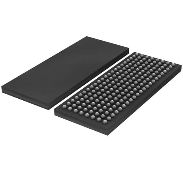
- Part No.:
- SSTUG32868ET/S,518
- Manufacturer:
- NXP Semiconductors
- Category:
- Specialty Logic
- Package:
- 176-TFBGA
- Datasheet:
-
 SSTUG32868ET/S,518.pdf
- Description:
- IC BUFFER 1.8V 25BIT 176-LFBGA
- Quantity:
- Payment:

- Shipping:

Inventory:2,890
Please send an inquiry. Send us your inquiry, and we will respond immediately.
Product details
Overview
SSTUG32868ET/S from NXP Semiconductors is a 1.8 V, 28-bit, 1:2 configurable registered buffer with integrated parity checking, designed specifically for DDR2-1G RDIMM applications. It integrates dual JEDEC-standard register functionality into one TFBGA176 package, supports up to 450 MHz operation, delivers high-output-drive strength, and features two additional chip select inputs (DCS2/DCS3) and open-drain QERR error reporting for memory subsystems in high-density server DIMMs.
For engineers reviewing the SSTUG32868ET/S datasheet, SSTUG32868ET/S pinout, SSTUG32868ET/S application, or SSTUG32868ET/S equivalent, key selection criteria include its 28-bit 1:2 register architecture, SSTL_18-compatible D-inputs, differential CK/CK clock interface, 0°C to +85°C industrial temperature range, and support for parity-enabled RDIMM designs requiring stub-series terminated logic compliance and low-power standby modes.
Technical Context
The SSTUG32868ET/S implements a dual-register architecture controlled by the LVCMOS C input, selecting between Register A (C = 0) and Register B (C = 1) configurations with distinct data channel mappings-e.g., D1–D5/D7/D9–D12/D17–D28 vs. D1–D12/D17–D20/D22/D24–D28. Its parity engine accepts PAR_IN one clock cycle after data, generates QERR two cycles later, and latches errors for ≥2 clock cycles or until RESET assertion.
It uses differential CK/CK inputs with 600 mV minimum VID and 0.675–1.125 V common-mode range, supports SSTL_18 data inputs (VIH(AC) = Vref + 0.25 V), and employs edge-controlled CMOS outputs optimized for unterminated DIMM loads. The device enables low-power active mode via CSGEN and four DCS inputs, gating Qn/QERR outputs when all are HIGH, while RESET retains priority to force outputs LOW and disable receivers.
Key Specifications
| Parameter | Value and Actual Design Meaning |
|---|---|
| Supply voltage | 1.7 V to 2.0 V nominal; enables stable operation across DDR2 VDD tolerance bands and simplifies power rail design in memory modules. |
| Max clock frequency | 450 MHz; supports DDR2-900 data rates (450 MT/s per pin) in registered DIMM applications. |
| Data width & ratio | 28-bit, 1:2 configurable register; re-drives each input to two independent output banks (QxA/QxB), enabling rank-level signal distribution. |
| Parity function | Even-parity checking across 22 DIMM-independent D-inputs; asserts open-drain QERR (active LOW) two clocks after error detection. |
| Output drive | Permanently configured high-output-drive strength; maintains signal integrity under heavy net loading in dense 2R×4 RDIMM layouts. |
| Package | TFBGA176, 6 mm × 15 mm, 0.65 mm pitch; provides compact footprint with adequate escape routing for high-speed DDR2 trace fanout. |
| Operating temperature | 0 °C to +85 °C; qualified for industrial-grade server memory module environments where thermal margin exceeds commercial-grade limits. |
Pinout & Package
Package: 176-ball thin fine-pitch ball grid array (TFBGA), 8 × 22 grid, 0.65 mm ball pitch, 6 mm × 15 mm body size, 0.7 mm height. Compatible with standard PCB assembly processes and provides thermal/mechanical reliability for memory module use.
| Pin/Terminal | Circuit Role | Design Meaning |
|---|---|---|
| D1–D28 | SSTL_18 data inputs | 28 parallel DDR2 command/address/data inputs clocked on CK/CK crossing; mapped differently per Register A/B configuration. |
| Q1A–Q28A / Q1B–Q28B | CMOS re-driven outputs | Two independent 28-bit output banks; each gated by DCS0/DCS1; used for rank-A/rank-B signal distribution on 2R×4 DIMMs. |
| CK / CK | Differential clock inputs | Master clock pair with 600 mV min differential swing and 0.675–1.125 V common-mode range; meets DDR2 timing jitter requirements. |
| PAR_IN | SSTL_18 parity input | Accepts even-parity bit one clock cycle after corresponding D-inputs; enables end-to-end error detection in memory controller-to-DIMM path. |
| QERR | Open-drain error output | Active-LOW error flag latched for ≥2 clock cycles; drives external pull-up for system-level parity fault signaling without level-shifting. |
| DCS0–DCS3 | SSTL_18 chip select inputs | Four independent enables; DCS0/DCS1 control Qn gating; DCS2/DCS3 extend JEDEC compatibility for advanced RDIMM decoding schemes. |
| C | LVCMOS configuration input | Selects Register A (C = LOW) or Register B (C = HIGH); hard-wired at board level to fix pinout mapping for target DIMM layout. |
| RESET | LVCMOS asynchronous reset | Forces all registers and outputs LOW (except QERR HIGH); disables differential receivers during power-up or fault recovery. |
| VREF | Reference voltage input | 0.9 V nominal reference for SSTL_18 input thresholding; two pins (A5/AB5) internally tied; only one requires external connection. |
| VDD / GND | Power supply terminals | 36 dedicated VDD balls and 40+ GND balls distributed across package; ensures low-impedance power delivery and noise suppression for high-speed switching. |
Key Features
| Feature | Design Value |
|---|---|
| Integrated dual-register functionality | Replaces two discrete JEDEC-standard DDR2 registers (e.g., SSTUA32864/SSTUA32866) in one TFBGA176 package, reducing PCB area and interconnect complexity. |
| Configurable 1:2 register mapping | Pinout reconfiguration via C input enables optimization for different DIMM topologies-Register A for legacy 2R×4, Register B for enhanced channel allocation. |
| On-die parity checking | Real-time even-parity validation across 22 D-inputs with QERR assertion two clocks post-data, eliminating need for external parity logic in RDIMM BOM. |
| High-output-drive strength | Permanently enabled drive capability maintains signal rise/fall times <4 V/ns and propagation delay ≤1.4 ns under heavy DIMM net loading conditions. |
| Four-chip-select support | DCS0–DCS3 inputs allow flexible rank/command decode in multi-rank RDIMMs while maintaining backward compatibility with JEDEC-standard register protocols. |
| Low-power standby mode | CSGEN + DCS0 + DCS1 HIGH disables Qn/QERR state changes, reducing dynamic current to ≤2 mA static standby without compromising error detection readiness. |
Applications
| Server Memory Modules | Enterprise Storage Controllers |
|---|---|
Use Scenario: High-density 2R×4 DDR2 RDIMMs deployed in 1U/2U rack servers supporting up to 32 GB per slot. IC Role / Device Role / Timing Role: Registered buffer managing address/command distribution to two DRAM ranks with parity-checked control path and sub-1.5 ns CK-to-Q propagation. Use Value: Enables reliable 450 MT/s operation in thermally constrained server chassis by integrating dual-register logic, parity, and high-drive outputs in one package. | Use Scenario: RAID controller memory subsystems requiring ECC-capable DIMMs with deterministic error reporting for data integrity verification. IC Role / Device Role / Timing Role: Parity-aware register ensuring command integrity from host controller to DRAM; QERR signals parity faults to BMC/IPMI firmware within two clock cycles. Use Value: Eliminates external parity logic, reduces BOM count by one IC, and provides hardware-accelerated fault detection without software overhead. |
| Telecom Baseband Units | Industrial Computing Platforms |
Use Scenario: Carrier-grade baseband units using DDR2 RDIMMs for packet buffering and signal processing with extended temperature operation. IC Role / Device Role / Timing Role: Temperature-hardened (0°C to +85°C) register providing robust clock-domain crossing and signal re-driving across long DIMM traces in conduction-cooled enclosures. Use Value: Maintains timing margins at 450 MHz across full industrial temp range, avoiding derating or derating-induced bandwidth loss in mission-critical telecom infrastructure. | Use Scenario: Ruggedized industrial PCs and programmable logic controllers using DDR2 RDIMMs in factory automation systems with variable ambient temperatures. IC Role / Device Role / Timing Role: Low-power active-mode register minimizing idle current (<2 mA standby) while retaining fast wake-up (<10 ns tACT) for deterministic real-time response. Use Value: Extends system uptime in uncooled deployments by reducing register quiescent power by >95% versus always-on alternatives. |
Equivalent & Alternatives
The following parts are listed as comparable options for similar DDR2 registered buffer applications.
| Alternative Part | Technical Difference | Application Difference | Selection Advice |
|---|---|---|---|
| IDT72V2851LPG | 28-bit 1:2 register without parity; operates at 1.8 V but lacks QERR output and PAR_IN interface. | Requires external parity logic for RDIMMs needing error detection; suitable only for non-parity DDR2 modules. | Select when parity is not required and JEDEC-compliant pinout is prioritized over integrated diagnostics. |
| ON Semiconductor NB3N551DR2G | 24-bit DDR2 register with parity; supports 400 MHz max clock; uses 144-ball TFBGA (smaller footprint but fewer I/Os). | Limited to 24-bit data paths; insufficient for full 28-bit DDR2 command/address bus in 2R×4 RDIMMs. | Choose only for space-constrained designs accepting reduced channel count or partial bus registration. |
Compared with IDT72V2851LPG and NB3N551DR2G, the SSTUG32868ET/S uniquely combines full 28-bit 1:2 registration, on-die even-parity checking with QERR, 450 MHz capability, and four-chip-select support-making it the only drop-in solution for high-reliability DDR2-1G RDIMMs requiring integrated error detection and industrial temperature operation.
Availability
SSTUG32868ET/S is available at Aetrix Electronics and suitable for server memory modules, enterprise storage controllers, and telecom baseband units requiring stable component supply, extended temperature performance (0°C to +85°C), and JEDEC-compliant DDR2 registered buffer functionality with integrated parity checking.
Supply support for SSTUG32868ET/S includes scheduled delivery planning, volume procurement assistance, BOM continuity management, traceable sourcing, and lifecycle availability coordination for OEM customers, industrial embedded developers, connected-device designers, and electronics production programs.
Manufacturer
NXP Semiconductors is a global semiconductor company headquartered in Eindhoven, Netherlands, specializing in secure connectivity solutions for automotive, industrial, and communication markets.
The SSTUG32868ET/S belongs to NXP's SSTU family of DDR2 registered buffers, engineered specifically for high-density RDIMM applications demanding integrated parity, high-speed timing, and industrial-grade thermal reliability in server and infrastructure platforms.
FAQ
What is the operating temperature range of the SSTUG32868ET/S?
The SSTUG32868ET/S is rated for operation from 0 °C to +85 °C ambient temperature, making it suitable for industrial and enterprise server environments where commercial-grade (0°C to +70°C) parts may fail under thermal stress. This extended range is confirmed in Table 2 of the official NXP datasheet and applies specifically to the /S suffix variant.
How does the C input affect the pin configuration of the SSTUG32868ET/S?
The C input selects between Register A (C = LOW) and Register B (C = HIGH) configurations, altering which D-inputs feed which Q-output banks-for example, Register A uses D1–D5/D7/D9–D12/D17–D28, while Register B uses D1–D12/D17–D20/D22/D24–D28. The C pin must be hard-wired and not toggled during operation, as stated in Section 7.2 of the datasheet.
Does the SSTUG32868ET/S support parity checking, and how is it implemented?
Yes, the SSTUG32868ET/S implements even-parity checking across 22 DIMM-independent D-inputs. It accepts PAR_IN one clock cycle after the associated data, compares it internally, and asserts the open-drain QERR output (active LOW) two clock cycles later. The error remains latched for ≥2 clock cycles or until RESET is asserted, per Tables 4 and 5 in the datasheet.
What package type and ball count does the SSTUG32868ET/S use?
The SSTUG32868ET/S uses a 176-ball thin fine-pitch ball grid array (TFBGA) package with an 8 × 22 grid, 0.65 mm ball pitch, and 6 mm × 15 mm body dimensions (SOT932-1). This is explicitly defined in Table 1 of the NXP datasheet and confirmed in Figures 3–5 showing ball mapping for both Register A and Register B modes.
Can the SSTUG32868ET/S operate at DDR2-900 speed (450 MHz clock)?
Yes, the SSTUG32868ET/S supports a maximum clock frequency of 450 MHz, as specified in Table 9 (fclk = 450 MHz) and Table 10 (fclk(max) = 450 MHz). This enables full DDR2-900 operation (450 MT/s per pin) in registered DIMM applications, provided setup/hold timing (tsu = 0.5 ns, th = 0.4 ns) and load conditions are met.
SSTUG32868ET/S,518 Specifications
- Product attributes
- Attribute value
- Manufacturer:
- NXP Semiconductors
- Series:
- -
- Package/Case:
- 176-TFBGA
- Packaging:
- Tape & Reel (TR)
- Product Status:
- Obsolete
- Logic Type:
- 1:2 Configurable Registered Buffer with Parity
- Supply Voltage:
- 1.7V ~ 2V
- Number of Bits:
- 28
- Operating Temperature:
- 0°C ~ 85°C
- Grade:
- -
- Qualification:
- -
- Mounting Type:
- Surface Mount
- Supplier Device Package:
- 176-TFBGA (15x6)
SSTUG32868ET/S,518 FAQ
1.How can I place an order for SSTUG32868ET/S,518 through Aetrix?
Please submit a Request for Quotation (RFQ) for SSTUG32868ET/S,518 on Aetrix. Our sales agent will provide a competitive quotation and guide you through the order confirmation once you accept the terms.
2.Are the price and stock information for SSTUG32868ET/S,518 reliable?
The price and inventory of SSTUG32868ET/S,518 are updated periodically and may fluctuate due to market conditions. Stock and pricing data are typically refreshed every 24 hours. Quotation validity for SSTUG32868ET/S,518 is usually 5 days.
3.What payment methods are accepted for SSTUG32868ET/S,518?
We accept Wire Transfer, PayPal, Credit Card, Western Union, MoneyGram, and Escrow for SSTUG32868ET/S,518 transactions.
Note: Certain payment methods may incur a processing fee.
4.How is shipping managed for SSTUG32868ET/S,518?
SSTUG32868ET/S,518 orders can be shipped via leading logistics carriers, including DHL, UPS, FedEx, TNT, or Registered Mail.
Once your SSTUG32868ET/S,518 order is processed, you will receive an email with the shipment details and tracking number.
Note: Tracking information may take up to 24 hours to appear. Express delivery typically takes 3–5 business days.
5.How can I obtain technical support or documentation for SSTUG32868ET/S,518?
For technical support, including SSTUG32868ET/S,518 datasheets, pinout diagrams, or application guidance, please contact our engineering support team. They can provide detailed documentation and assistance for your SSTUG32868ET/S,518 requirements.
6.How does Aetrix verify that SSTUG32868ET/S,518 is sourced from the original manufacturer or authorized distributors?
All SSTUG32868ET/S,518 products on Aetrix are procured from qualified distributors and authorized channels. Our dedicated quality assurance team conducts strict verification, including traceability checks and, if necessary, third-party testing. This ensures that SSTUG32868ET/S,518 meets industry standards.
7.What is the process for return or replacement of SSTUG32868ET/S,518?
All SSTUG32868ET/S,518 units undergo pre-shipment inspection (PSI). If there is an issue with SSTUG32868ET/S,518, returns or replacements are accepted under the following conditions:
1.Quantity discrepancies, incorrect items, or visible external defects (such as breakage or corrosion), acknowledged by Aetrix.
2.The issue is reported within 90 days of delivery.
3.The SSTUG32868ET/S,518 part is unused and in its original packaging.
Return procedure for SSTUG32868ET/S,518:
1.Submit a request within 90 days.
2.Obtain a Return Material Authorization (RMA) from Aetrix.
SSTUG32868ET/S,518 Tags

-
MC14490DWR2G
onsemi
-
SY58600UMG-TR
Microchip Technology

-
MC100EP16DTR2G
onsemi
-
MC100EP16MNR4G
onsemi
-
74LVC1GX04GW,125
Nexperia USA Inc.

-
CD4007UBE
Texas Instruments
-
NXS0104PWJ
Nexperia USA Inc.

-
CD74HC283M96
Texas Instruments

-
SN74LVC1GX04DCKR
Texas Instruments

-
SN74F283N
Texas Instruments
-
SN74LVC1404DCTR
Texas Instruments

-
SN74LVC1GX04DBVR
Texas Instruments
Tech Hub

A practical engineering guide to 3.3V and 5V logic compatibility, input thresholds, resistor dividers, translator ICs, MOSFET level shifting, I2C pull-ups, timing limits and power-sequencing risks.

The 74HC595 uses push-pull logic outputs, while the TPIC6B595 uses 50 V open-drain DMOS sinks for higher-power loads. This guide compares timing, current limits, 3.3 V interfacing, load wiring, thermal…

The 74HC595 converts serial data into eight stable parallel outputs. This guide covers pin functions, shift and storage timing, OE and MR behavior, drive-current limits, cascading, voltage compatibilit…

A technical comparison of level-sensitive latches and edge-triggered flip-flops, covering timing windows, setup and hold limits, master–slave operation, time borrowing, race-through, HDL inference and…

A D latch stores one bit while Enable controls when data can pass. This reference covers gate-level operation, truth tables, transparency, setup and hold timing, LE versus OE, common ICs and practical …

An SR latch stores one bit through cross-coupled feedback. This engineering reference covers NOR and NAND implementations, truth tables, forbidden-state recovery, gated operation, switch debouncing, fa…

Latch circuits retain one bit through feedback. This technical reference covers SR and D latches, truth tables, transparency, timing limits, latch-versus-flip-flop behavior, applications and common log…

An engineering guide to LED driver operation, constant-current and constant-voltage outputs, linear and switching topologies, dimming, IC selection, calculations, replacement compatibility, and fault c…

Operational amplifier guide covering op amp basics, feedback, ideal vs real op amps, common configurations, buffer circuits, offset, bias current, gain-bandwidth, slew rate, rail-to-rail limits and sel…

Jumper cables guide covering safe connection order, red and black clamp placement, final ground connection, cable gauge, length, clamp quality, copper vs CCA cables, jump starter comparison and battery…


