
 My Inquiry
 My Account


STMicroelectronics ST7590T
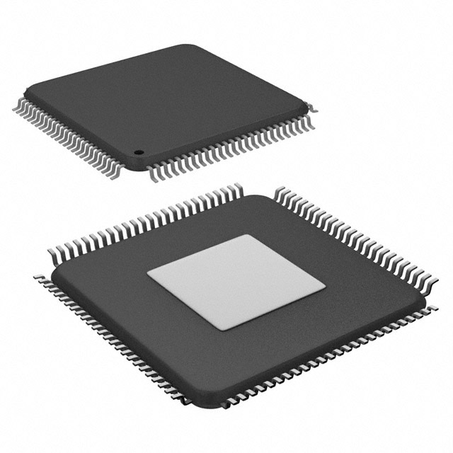
- Part No.:
- ST7590T
- Manufacturer:
- STMicroelectronics
- Category:
- Telecom
- Package:
- 100-TQFP Exposed Pad
- Datasheet:
-
 ST7590T.pdf
- Description:
- IC TELECOM INTERFACE 100TQFP
- Quantity:
- Payment:

- Shipping:

Inventory:2,052
Please send an inquiry. Send us your inquiry, and we will respond immediately.
Product details
Overview
ST7590T from STMicroelectronics is a narrow-band OFDM power line networking system-on-chip designed for PRIME-compliant smart metering and smart grid communication nodes. The IC integrates a DSP-based PHY processor, embedded 8051 protocol controller, analog front end, ADC, DAC, programmable gain receiver, high-linearity transmitter, integrated power amplifier, AES-128 hardware block, zero-crossing detector, clock management, and digital host interfaces.
For engineers reviewing the ST7590T datasheet, ST7590T pinout, ST7590T application, or ST7590T equivalent, this PLC SoC is most relevant for PRIME PHY power line communication, CENELEC A-band smart-meter networks, AMR / AMI concentrator and node designs, mains-line data communication, and external-memory PLC implementations requiring a TQFP100 exposed-pad package, 8 V to 18 V line-driver supply, 3.3 V or 5 V digital I/O, UART / SPI host control, and external serial nonvolatile memory support.
Technical Context
ST7590T implements a PRIME-compliant OFDM physical layer with 96 subcarriers in the CENELEC A band. It supports BDPSK, QDPSK, and 8DPSK programmable modulation, convolutional coding, Viterbi decoding, signal-to-noise ratio estimation, channel-quality estimation, and programmable bit rate up to 128 kbps, giving smart-grid PLC nodes a complete digital modem and protocol-processing base.
In the TQFP100 package option, ST7590T uses dedicated firmware implementing the PRIME-compliant PHY protocol layer and a boot-loader procedure that allows PRIME MAC, PRIME CL432 convergence layer, and IEC 61334-4-32 LLC layer code to boot from external serial nonvolatile memory through the SPI interface. The 100-pin package also exposes an external SRAM controller, allowing program-code execution from optional parallel SRAM when the system architecture requires it.
Key Specifications
| Parameter | Value and Actual Design Meaning |
|---|---|
| Device Type | Narrow-band OFDM power line networking system-on-chip for PRIME-compliant smart metering and smart grid PLC communication. |
| Protocol / PHY Context | Full PRIME-compliant PHY with OFDM modulation and embedded firmware support for PRIME-based power line communication systems. |
| OFDM Structure | 96 subcarriers in the CENELEC A band, supporting power line data communication for automatic meter reading and smart-grid networks. |
| Modulation | BDPSK, QDPSK, and 8DPSK programmable modulation, allowing different robustness and throughput settings according to channel quality. |
| Maximum Bit Rate | Programmable bit rate up to 128 kbps for PRIME PLC data communication. |
| Digital Architecture | DSP engine, PHY processor, hardware accelerators, embedded 8051 controller core, watchdog, timers, interrupts, and protocol controller resources. |
| Security Function | On-chip AES-128 hardware block for secure PRIME communication handling. |
| Analog Front End | Integrated ADC, DAC, programmable gain receiver, automatic gain behavior, high-linearity transmitter, and power amplifier interface. |
| Power Amplifier | Integrated power line driver delivers up to 1 Arms typical output current and 14 Vpp single-ended output capability, supporting low-impedance PLC line conditions. |
| Receiver Path | Receiver input supports up to 16 Vpp maximum input range at the lowest PGA gain; PGA gain range is -18 dB to +30 dB in 6 dB typical steps. |
| Transmitter Path | DAC-based transmit path with digital gain range from -21 dB to 0 dB in 3 dB typical steps for PRIME output-level control. |
| Host Interface | UART / SPI0 host-controller interface using MOSI0_TXD, MISO0_RXD, SCLK0, and SSN0 functions. |
| External Memory Interface | SPI1 / I²C serial memory interface and parallel SRAM controller available in the TQFP100 version for external NVM and optional SRAM use. |
| Clock Requirement | 8 MHz crystal connected to XIN / XOUT or an 8 MHz external clock supplied directly to XIN. |
| Supply Rails | 8 V to 18 V VCC main supply for the line-driver section and 3.3 V or 5 V VDDIO supply for digital I/O; internal regulators generate 5 V analog and 1.8 V core-related rails. |
| Temperature Range | -40°C to +85°C operating ambient temperature range for industrial smart-metering equipment. |
| ESD Rating | ±2 kV human-body-model ESD robustness under the listed qualification condition. |
| Package | TQFP100 exposed-pad package, 14 mm × 14 mm body, 0.50 mm pitch, supplied as ST7590T in tray packaging. |
Pinout & Package
ST7590T is supplied in a TQFP100 exposed-pad package with a 14 mm × 14 mm body, 16 mm × 16 mm nominal overall lead span, 0.50 mm lead pitch, and low-profile 1.2 mm maximum package height. The exposed-pad TQFP format gives the TQFP100 version enough pins for the external SRAM bus, serial memory interface, host interface, PLC analog front end, power amplifier pins, zero-crossing detector, oscillator, JTAG, GPIO, and multiple power domains used in a complete PRIME PLC node.
| Pin / Terminal | Circuit Role | Design Meaning |
|---|---|---|
| MOSI0_TXD, MISO0_RXD, SCLK0, SSN0 | UART / SPI0 host communication interface. | Provides the main digital communication path between ST7590T and the host controller for command, data, and protocol-control traffic. |
| MISO1, MOSI1_SDA, SCLK1_SCL | SPI1 / I²C serial memory interface pins. | Connect external serial nonvolatile memory used by the TQFP100 version to boot PRIME MAC, convergence-layer, and LLC-related firmware code. |
| SRAM_A0 to SRAM_A16 | External SRAM address bus. | Provides address outputs for optional parallel SRAM used for external program-code execution in ST7590T-based PLC systems. |
| SRAM_D0 to SRAM_D7 | External SRAM data bus. | Provides the bidirectional 8-bit data interface for optional external SRAM connection. |
| SRAM_CSN, SRAM_WEN, SRAM_OEN | External SRAM control pins. | Control chip-select, write-enable, and output-enable timing for the optional asynchronous SRAM memory interface. |
| TX_OUT | Transmission analog output. | Provides the DAC-based transmit signal before the external active-filter or power-amplifier feedback network. |
| PA_IN_P, PA_IN_N | Differential power amplifier inputs. | Feed the integrated power amplifier section used to drive the PLC coupling network. |
| PA_OUT | Power amplifier output. | Drives the external power line coupling and active-filter network, supporting high-current transmission into the mains-coupling interface. |
| CL | Current limiting feedback input. | Monitors output-current feedback for the integrated power amplifier current-control function. |
| RX_IN | Reception analog input. | Receives the coupled PLC signal from the power line interface and feeds the programmable-gain receiver and ADC path. |
| ZC_IN | Zero-crossing detection input. | Connects to the mains zero-crossing conditioning circuit and provides timing information used by PRIME communication management. |
| XIN, XOUT | 8 MHz crystal oscillator pins. | Connect an 8 MHz crystal or provide an external 8 MHz clock to XIN for internal digital and PLC timing generation. |
| GPIO0 to GPIO9 | General-purpose digital I/O pins. | Provide configurable digital signaling for PLC activity indication, host-control support, board-status functions, and system integration. |
| TDI, TDO, TCK, TMS, TRSTN | JTAG interface pins. | Provide system / 8051 core debug and test access through the JTAG interface. |
| RESETN | Active-low system reset input. | Resets the internal digital system and is normally driven by the host controller or board reset circuitry. |
| VCC, VSS | Main power amplifier supply and power ground. | Supply the line-driver section from the 8 V to 18 V power rail and provide the high-current return path for PLC transmission. |
| VDDIO, VDD, VDD_PLL, VDD_REG_1V8 | Digital I/O, digital core, PLL, and regulator-related supply pins. | Separate power domains support 3.3 V or 5 V I/O operation and 1.8 V internal digital / PLL filtering requirements. |
| VCCA, VSSA, VSUBS | Analog supply and analog ground pins. | Support the analog front end, receiver, transmitter, oscillator-related analog blocks, and substrate / analog grounding structure. |
| VDD_12V | OTP programming voltage pin. | Provides the 12 V programming supply path associated with the embedded OTP memory function. |
Key Features
- Fully integrated narrow-band OFDM power line networking SoC for PRIME-compliant PLC nodes.
- 96 OFDM subcarriers in the CENELEC A band with BDPSK, QDPSK, and 8DPSK programmable modulation.
- Programmable data rate up to 128 kbps with convolutional coding and Viterbi decoding.
- DSP engine, embedded 8051 controller, hardware accelerators, timers, watchdog, GPIO, interrupts, and protocol-control resources.
- Integrated ADC, DAC, programmable-gain receiver, high-linearity transmitter, and power amplifier for a complete PLC analog front end.
- Integrated power amplifier delivering up to 1 Arms typical output current and 14 Vpp single-ended output swing.
- Host UART / SPI interface plus serial external memory interface and external SRAM controller in the TQFP100 package option.
- On-chip AES-128 hardware block, zero-crossing detector, temperature sensor, power-management functions, and 8 MHz oscillator support.
- 8 V to 18 V line-driver supply, 3.3 V or 5 V digital I/O supply, and -40°C to +85°C operating temperature range.
Applications
| PRIME Smart Metering Nodes | AMR / AMI Power Line Networks |
|---|---|
|
Use Scenario: Electricity meters and smart-meter communication nodes using PRIME-compliant PLC over the mains line. IC Role: Narrow-band OFDM PLC SoC integrating the PRIME PHY, analog front end, line driver, host interface, and memory-boot structure. Use Value: ST7590T combines the modem, AFE, and power amplifier functions needed to build compact mains-coupled metering communication hardware. |
Use Scenario: Automatic meter reading and advanced metering infrastructure systems that communicate through existing low-voltage power lines. IC Role: PLC transceiver and protocol-processing IC with CENELEC A-band OFDM communication capability. Use Value: Up to 128 kbps PRIME data communication and channel-quality estimation support robust remote metering links over noisy mains wiring. |
| Smart Grid Data Concentrators | PLC Reference and Industrial Control Nodes |
|
Use Scenario: Smart grid equipment collecting and routing PRIME PLC data between meter nodes and higher-level communication systems. IC Role: Power line networking SoC with external serial NVM boot and optional SRAM execution support in the TQFP100 version. Use Value: External memory support gives system designers more flexibility for protocol-layer code, updates, and node-role implementation. |
Use Scenario: Industrial and utility equipment requiring narrow-band communication over existing power wiring. IC Role: Integrated PLC modem with AFE, transmit amplifier, receive PGA, zero-crossing detector, and host-controller communication. Use Value: The integrated line driver, analog receive path, and host interface reduce external PLC signal-chain complexity while supporting regulatory-oriented line-coupling design. |
Equivalent & Alternatives
When evaluating ST7590T equivalent devices, engineers should compare PLC protocol support, OFDM modulation, external memory requirements, package footprint, power amplifier capability, line-coupling topology, host-interface behavior, software stack, supply rails, temperature range, and whether the design requires pin compatibility or a redesigned PLC modem architecture.
| Alternative Part | Technical Difference | Application Difference | Selection Advice |
|---|---|---|---|
| ST7590TR | Same ST7590T TQFP100 exposed-pad package and PRIME PLC SoC architecture, but supplied in tape-and-reel format rather than tray-oriented handling. | Used when the same PCB, pinout, and firmware architecture must be retained but automated SMT production requires reel-fed logistics. | Select ST7590T for tray-based sourcing or service needs; select ST7590TR when the same TQFP100 circuit requires tape-and-reel assembly flow. |
| ST7590 | Same ST7590 family in QFN48 7 mm × 7 mm package; the QFN48 version includes firmware for the full PRIME protocol stack and does not expose the same external memory bus as the TQFP100 version. | Better suited for compact PLC nodes where the embedded full-stack ROM approach and smaller QFN48 footprint match the system architecture. | Select ST7590T when the design requires TQFP100 external memory support; select ST7590 only when the PCB, firmware architecture, and QFN48 package design are matched to that version. |
| ST8500TR | Later ST power line communication modem SoC family member with a different architecture, package, firmware environment, and design ecosystem from ST7590T. | Relevant for redesigned PLC products where maintaining ST7590T pinout and legacy PRIME implementation is not required. | Use ST8500TR as a redesign comparison option; keep ST7590T when the existing PCB, external-memory boot structure, TQFP100 footprint, and ST7590 software environment must remain unchanged. |
Compared with ST7590, ST7590T is optimized for the TQFP100 implementation with external serial NVM boot support and optional external SRAM interface access. ST7590T vs ST7590TR selection is mainly a packaging-logistics decision, while ST7590T vs ST8500TR selection requires a broader review of hardware redesign, protocol stack, firmware migration, line-coupling design, and product lifecycle requirements.
Quality
ST7590T should be sourced as original STMicroelectronics components through traceable and controlled supply channels. Quality verification procedures may include TQFP100 exposed-pad package inspection, top-mark validation, tray and label review, lead coplanarity inspection, solderability testing, VCC / VDDIO continuity checks, oscillator startup verification, host UART / SPI communication testing, external memory interface checks, PLC transmit / receive path screening, PA_OUT bias inspection, and incoming inspection according to smart-metering PLC production requirements.
Availability
ST7590T is available at Aetrix Electronics and suitable for PRIME smart-metering nodes, AMR / AMI communication modules, power line networking equipment, smart grid PLC boards, and legacy ST7590T-based utility products requiring stable component supply and repeatable production support.
Supply support may include scheduled delivery planning, volume procurement support, BOM continuity assistance, traceable sourcing management, and long-term availability support for meter manufacturers, utility equipment builders, PLC module developers, repair groups, contract manufacturers, and legacy smart-grid product owners.
For production deployment, confirming the TQFP100 exposed-pad footprint, external serial NVM requirement, optional SRAM bus use, 8 MHz clock plan, 8 V to 18 V VCC supply, 3.3 V or 5 V VDDIO interface level, PLC coupling-network design, host interface mode, environmental requirements, and sourcing continuity helps reduce procurement risk and improve manufacturing stability.
Manufacturer
STMicroelectronics supplies power line communication transceivers, microcontrollers, connectivity devices, analog ICs, power-management components, sensors, protection products, and discrete semiconductors for smart energy, industrial, automotive, communication, and embedded applications. ST7590T belongs to ST's STarGRID power line networking portfolio for PRIME-compliant narrow-band OFDM PLC communication.
FAQ
What is ST7590T used for?
ST7590T is used for narrow-band OFDM power line communication in PRIME-compliant smart metering, AMR / AMI networks, smart grid nodes, and utility communication equipment. It integrates the PLC physical layer, analog front end, line driver, host interface, encryption block, zero-crossing detector, and memory-boot support needed for mains-line data communication.
What communication standard does ST7590T support?
ST7590T supports PRIME-compliant power line communication using OFDM with 96 subcarriers in the CENELEC A band. The PHY supports BDPSK, QDPSK, and 8DPSK modulation, plus convolutional coding, Viterbi decoding, signal-to-noise estimation, and channel-quality estimation for operation over noisy low-voltage power networks.
What is the difference between ST7590T and ST7590?
ST7590T is the TQFP100 package version with external serial nonvolatile memory boot support and optional external SRAM interface access. ST7590 is the QFN48 version, which uses embedded firmware for the full PRIME protocol stack and does not provide the same external memory bus structure. The two versions require different PCB layouts and firmware-memory planning.
What package is used by ST7590T?
ST7590T uses a TQFP100 exposed-pad package with a 14 mm × 14 mm body, 0.50 mm pitch, and 1.2 mm maximum height. The 100-pin package exposes host interface pins, external memory pins, analog PLC pins, power amplifier pins, GPIO, JTAG, oscillator pins, and multiple supply domains needed by a complete PLC node.
Which supplies are required by ST7590T?
ST7590T uses an 8 V to 18 V VCC supply for the main power-line driver section and a 3.3 V or 5 V VDDIO supply for digital I/O. Internal regulators generate the 5 V analog supply and 1.8 V digital / PLL-related rails, and those regulator outputs are used for filtering rather than for powering external circuitry.
Does ST7590T include a power amplifier?
Yes. ST7590T includes an integrated power amplifier for power line transmission. The amplifier supports up to 1 Arms typical output current and 14 Vpp single-ended output capability, and its PA_IN_P, PA_IN_N, PA_OUT, and CL pins allow the external active-filter and current-feedback network to be designed around the required line-coupling interface.
What clock does ST7590T need?
ST7590T uses an 8 MHz clock source. The design can connect an 8 MHz crystal between XIN and XOUT, with the internal oscillator using integrated load-capacitor support, or it can drive XIN directly with an external 8 MHz clock while leaving XOUT unused. Stable clock design is important for PLC modem timing and protocol operation.
What are common ST7590T alternatives?
Common comparison options include ST7590TR for the same TQFP100 PLC SoC in tape-and-reel format, ST7590 for the smaller QFN48 version with a different memory approach, and ST8500TR for a later ST power line communication modem redesign path. These options are not automatically interchangeable; engineers must compare package, firmware, memory interface, line coupling, and host software requirements.
ST7590T Specifications
- Product attributes
- Attribute value
- Manufacturer:
- STMicroelectronics
- Series:
- -
- Package/Case:
- 100-TQFP Exposed Pad
- Packaging:
- Tray
- Product Status:
- Active
- Function:
- Power Line Networking System-On-Chip
- Interface:
- I2C, SPI
- Number of Circuits:
- 1
- Voltage - Supply:
- 8V ~ 18V
- Current - Supply:
- -
- Power (Watts):
- -
- Operating Temperature:
- -40°C ~ 80°C
- Grade:
- -
- Qualification:
- -
- Mounting Type:
- Surface Mount
- Supplier Device Package:
- 100-TQFP (14x14)
ST7590T FAQ
1.How can I place an order for ST7590T through Aetrix?
Please submit a Request for Quotation (RFQ) for ST7590T on Aetrix. Our sales agent will provide a competitive quotation and guide you through the order confirmation once you accept the terms.
2.Are the price and stock information for ST7590T reliable?
The price and inventory of ST7590T are updated periodically and may fluctuate due to market conditions. Stock and pricing data are typically refreshed every 24 hours. Quotation validity for ST7590T is usually 5 days.
3.What payment methods are accepted for ST7590T?
We accept Wire Transfer, PayPal, Credit Card, Western Union, MoneyGram, and Escrow for ST7590T transactions.
Note: Certain payment methods may incur a processing fee.
4.How is shipping managed for ST7590T?
ST7590T orders can be shipped via leading logistics carriers, including DHL, UPS, FedEx, TNT, or Registered Mail.
Once your ST7590T order is processed, you will receive an email with the shipment details and tracking number.
Note: Tracking information may take up to 24 hours to appear. Express delivery typically takes 3–5 business days.
5.How can I obtain technical support or documentation for ST7590T?
For technical support, including ST7590T datasheets, pinout diagrams, or application guidance, please contact our engineering support team. They can provide detailed documentation and assistance for your ST7590T requirements.
6.How does Aetrix verify that ST7590T is sourced from the original manufacturer or authorized distributors?
All ST7590T products on Aetrix are procured from qualified distributors and authorized channels. Our dedicated quality assurance team conducts strict verification, including traceability checks and, if necessary, third-party testing. This ensures that ST7590T meets industry standards.
7.What is the process for return or replacement of ST7590T?
All ST7590T units undergo pre-shipment inspection (PSI). If there is an issue with ST7590T, returns or replacements are accepted under the following conditions:
1.Quantity discrepancies, incorrect items, or visible external defects (such as breakage or corrosion), acknowledged by Aetrix.
2.The issue is reported within 90 days of delivery.
3.The ST7590T part is unused and in its original packaging.
Return procedure for ST7590T:
1.Submit a request within 90 days.
2.Obtain a Return Material Authorization (RMA) from Aetrix.
ST7590T Tags

-
LMC567CMX/NOPB
Texas Instruments
-
LM567CMX/NOPB
Texas Instruments
-
LM567CM/NOPB
Texas Instruments

-
VSC8531XMW-02
Microchip Technology
-
VSC8531XMW-05
Microchip Technology

-
GPY115C0VI
MaxLinear, Inc.

-
SI32185-A-FMR
Skyworks Solutions Inc.

-
VSC8541XMV-05
Microchip Technology

-
SI32178-B-FM1R
Skyworks Solutions Inc.
-
GPY215C0VI
MaxLinear, Inc.

-
CPC7514ZTR
Littelfuse Inc.

-
VSC8502XML-03
Microchip Technology
Tech Hub

Counterfeit components can hide behind convincing markings and passing basic function tests. This engineering reference covers source traceability, external inspection, X-ray, XRF, electrical testing, …

A practical engineering and sourcing framework covering lifecycle verification, lifetime-buy calculations, replacement qualification, supplier checks and counterfeit-risk controls.

TTL and CMOS logic families differ in thresholds, loading, output drive, power and timing. This engineering guide compares 74HC and 74HCT, calculates noise margins and checks 3.3 V/5 V compatibility.

A practical engineering guide to 3.3V and 5V logic compatibility, input thresholds, resistor dividers, translator ICs, MOSFET level shifting, I2C pull-ups, timing limits and power-sequencing risks.

The 74HC595 uses push-pull logic outputs, while the TPIC6B595 uses 50 V open-drain DMOS sinks for higher-power loads. This guide compares timing, current limits, 3.3 V interfacing, load wiring, thermal…

The 74HC595 converts serial data into eight stable parallel outputs. This guide covers pin functions, shift and storage timing, OE and MR behavior, drive-current limits, cascading, voltage compatibilit…

A technical comparison of level-sensitive latches and edge-triggered flip-flops, covering timing windows, setup and hold limits, master–slave operation, time borrowing, race-through, HDL inference and…

A D latch stores one bit while Enable controls when data can pass. This reference covers gate-level operation, truth tables, transparency, setup and hold timing, LE versus OE, common ICs and practical …

An SR latch stores one bit through cross-coupled feedback. This engineering reference covers NOR and NAND implementations, truth tables, forbidden-state recovery, gated operation, switch debouncing, fa…

Latch circuits retain one bit through feedback. This technical reference covers SR and D latches, truth tables, transparency, timing limits, latch-versus-flip-flop behavior, applications and common log…


