
 My Inquiry
 My Account


STMicroelectronics STBC15LJTR
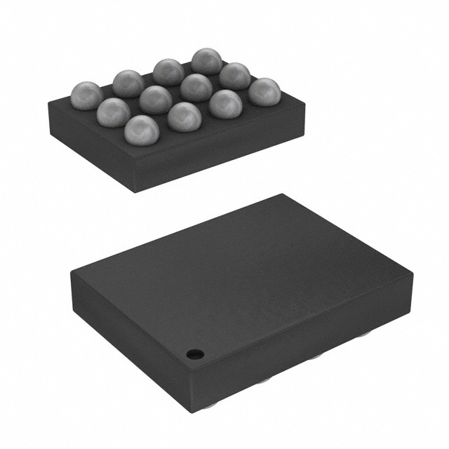
- Part No.:
- STBC15LJTR
- Manufacturer:
- STMicroelectronics
- Category:
- Battery Chargers
- Package:
- 12-XFBGA, FCBGA
- Datasheet:
-
 STBC15LJTR.pdf
- Description:
- IC BAT CHG LI-ION 1CL 12FLIPCHIP
- Quantity:
- Payment:

- Shipping:

Inventory:4,187
Please send an inquiry. Send us your inquiry, and we will respond immediately.
Product details
Overview
STBC15LJTR from STMicroelectronics is a linear lithium-ion battery charger IC optimized for ultra-low-power wearable and energy-harvesting systems. It delivers up to 40 mA charging current using CC-CV algorithm, supports programmable floating voltage (4.4 V typical), features 250 nA battery leakage current, reverse current protection, and shelf-mode operation consuming <10 nA. It targets thin-profile Li-Ion cells in fitness trackers and wireless sensor nodes.
For engineers reviewing the STBC15LJTR datasheet, STBC15LJTR pinout, STBC15LJTR application, or STBC15LJTR equivalent, key selection criteria include its Flip-chip12 package footprint, Li-Ion–optimized 4.4 V float voltage, peak-mode–enabled over-discharge threshold adjustment, and ultra-low quiescent current under no-input conditions.
Technical Context
The STBC15LJTR implements a dedicated CC/CV finite-state machine for Li-Ion charging without pre-charge or termination phases, relying on external pin configuration (VSET0/VSET1) to select one of four floating voltages (4.20–4.40 V). Its internal M3 transistor provides battery disconnection during over-discharge, with PKM input enabling dynamic lowering of VBAT_OVD from 2.7 V to 2.65 V.
Shelf-mode activation via SM pin disables all internal circuitry except a 100 kΩ pull-down, reducing total current draw to <10 nA; reverse current protection is enforced by turning off M1 when CHGIN falls below UVLO (6.5 V), preventing battery-to-source backflow-critical for photovoltaic energy harvesting inputs.
Key Specifications
| Parameter | Value and Actual Design Meaning |
|---|---|
| Charging Current | Selectable up to 40 mA via ISET0/ISET1 pins; enables precise matching to low-capacity Li-Ion cells (e.g., 10–50 mAh). |
| Floating Voltage | 4.40 V (typical, VSET0=VSET1=CHGIN); ±0.5% accuracy ensures cell longevity and cycle count optimization. |
| Battery Leakage | 250 nA max (VBAT > VBAT_OVD, CHGIN = 0 V); minimizes self-discharge during storage or idle periods. |
| Shelf-Mode Current | <10 nA (SM = high, VBAT = 4 V); eliminates need for mechanical battery disconnect in long-shelf-life devices. |
| Over-Discharge Threshold | 2.70 V (PKM = 0 or 1); fixed for STBC15L, prevents irreversible Li-Ion cell damage below safe voltage. |
| Input UVLO | 6.5 V rising threshold with 150 mV hysteresis; avoids erratic startup near USB 5 V or harvester output limits. |
| Package | Flip-chip12 (1.1 × 1.41 mm, 300 µm pitch); enables sub-2 mm² PCB area for space-constrained wearables. |
Pinout & Package
STBC15LJTR is supplied in Flip-chip12 package: 1.1 × 1.41 mm body, 300 µm bump pitch, 0.30 mm max height. Terminal A3 is marked by a circular clear area (~0.1 mm Ø); A1 is identified by a larger clear area (~0.5 mm Ø) on top surface.
| Pin/Terminal | Circuit Role | Design Meaning |
|---|---|---|
| CHGIN | Input supply voltage | Accepts 5 V USB or energy harvester output; bypassed with 10 µF ceramic capacitor for stability. |
| BAT | Battery positive terminal | Connects directly to Li-Ion anode; bypassed with 4.7 µF ceramic capacitor to suppress ripple. |
| OUT | System output rail | Supplies downstream MCU/sensor; requires 1 µF ceramic decoupling for load transient response. |
| GND | Ground reference | Common return for all power and signal paths; must be low-impedance connection to minimize noise. |
| VSET0, VSET1 | Floating voltage selection | Dual-pin binary encoding selects 4.20/4.25/4.35/4.40 V; no internal pull-up/down-must be hard-wired to CHGIN or GND. |
| ISET0, ISET1 | Charging current selection | Dual-pin binary encoding sets 10/20/30/40 mA; determines charge time and thermal budget for small cells. |
| PKM | Peak mode enable | Low-active input that reduces VBAT_OVD threshold to avoid false shutdown during RF burst loads. |
| PG | Power-Good open-drain | Signals valid OUT voltage (>4.1 V); requires external pull-up to OUT for system power sequencing. |
| CHGINOK | Input source status | Open-drain negated flag indicating CHGIN is above UVLO; used to disable charging when input fails. |
| SM | Shelf-mode activation | Active-high input with internal 100 kΩ pull-down; asserts shelf mode to reduce current to <10 nA. |
Key Features
| Feature | Design Value |
|---|---|
| Programmable CC-CV charging | Four discrete current levels (10–40 mA) and four float voltages (4.20–4.40 V) set via dedicated pins-no I²C or firmware required. |
| Ultra-low shelf-mode current | <10 nA consumption with SM high enables multi-year shelf life without battery replacement or mechanical switch. |
| Li-Ion–optimized protection | Dedicated 2.7 V over-discharge cutoff and 4.1 V reconnection hysteresis prevent deep discharge and ensure reliable restart after load removal. |
| Reverse current blocking | M1 FET automatically disables when CHGIN drops below 6.5 V, eliminating external diode and protecting harvester sources like solar cells. |
| Peak-mode adaptive cutoff | PKM pin lowers VBAT_OVD to 2.65 V only during high-current transients-preserves runtime while avoiding false shutdowns. |
Applications
| Fitness Wearables | Energy Harvesting Nodes |
|---|---|
Use Scenario: Continuous heart-rate monitoring in compact wristband with integrated solar cell. IC Role / Device Role / Timing Role: Linear Li-Ion charger managing intermittent 50–200 µW solar input to maintain 25 mAh battery at 4.4 V float. Use Value: Shelf-mode <10 nA prevents >1% annual self-discharge; PKM avoids shutdown during BLE advertising bursts. | Use Scenario: Self-powered industrial vibration sensor powered by piezoelectric harvester. IC Role / Device Role / Timing Role: Energy buffer manager converting sporadic µW–mW harvest pulses into stable 3.3 V system rail via BAT/OUT path. Use Value: Reverse current blocking protects harvester from battery backfeed; 250 nA leakage preserves stored charge between harvest events. |
| Smart Cards | Wireless Medical Sensors |
Use Scenario: Contactless payment card with embedded Li-Ion battery recharged during NFC field exposure. IC Role / Device Role / Timing Role: Ultra-small-footprint charger (Flip-chip12) accepting brief 5 V NFC-induced pulses to top up 10 mAh cell. Use Value: 1.1 × 1.41 mm package fits within ISO 7816 card thickness; 40 mA fast-charge capability maximizes energy capture per field event. | Use Scenario: Disposable glucose monitor worn for 7 days, recharged via USB before reuse. IC Role / Device Role / Timing Role: Safety-compliant Li-Ion charger enforcing 4.4 V float and over-discharge cutoff to meet ISO 13485 battery requirements. Use Value: Fixed 2.7 V VBAT_OVD prevents cell degradation; 0.5% float voltage accuracy ensures consistent capacity across production units. |
Equivalent & Alternatives
The following parts are listed as comparable options for similar linear Li-Ion charging applications.
| Alternative Part | Technical Difference | Application Difference | Selection Advice |
|---|---|---|---|
| BQ25504RGET | Integrated boost converter + LDO; 150 nA quiescent current; 4.2 V fixed float; no shelf-mode pin. | Requires higher input voltage (>1.8 V); suited for thermoelectric or RF harvesters, not USB direct charge. | Choose if boosting low-voltage harvesters is needed; avoid if USB 5 V input and shelf-mode are mandatory. |
| MAX17320G+T | Smart fuel gauge + charger in WLP-20; 1.2 µA sleep current; I²C programmable; 4.2 V float only. | Enables state-of-charge reporting but adds firmware dependency and larger 2.1 × 2.1 mm footprint. | Choose if battery telemetry is required; avoid if minimal BOM and zero-code operation are design priorities. |
Compared with BQ25504RGET and MAX17320G+T, STBC15LJTR offers the smallest footprint (1.1 × 1.41 mm), lowest shelf-mode current (<10 nA), and pin-strapped configurability-making it optimal for cost-sensitive, space-constrained, firmware-free Li-Ion charging in wearables and disposable sensors.
Availability
STBC15LJTR is available at Aetrix Electronics and suitable for fitness wearables, energy harvesting nodes, smart cards, and wireless medical sensors requiring stable component supply, long shelf life, and ultra-low-power Li-Ion charging.
Supply support for STBC15LJTR includes scheduled delivery planning, volume procurement assistance, BOM continuity management, traceable sourcing, and lifecycle availability coordination for OEM customers, industrial embedded developers, connected-device designers, and electronics production programs.
Manufacturer
STMicroelectronics is a global semiconductor leader headquartered in Geneva, Switzerland, designing and manufacturing microcontrollers, analog ICs, power management, and MEMS sensors for industrial, automotive, and consumer markets.
The STBC15 product line delivers ultra-low-quiescent linear chargers specifically for micro-energy applications-targeting thin-film and Li-Ion batteries in energy-constrained IoT endpoints where size, leakage, and shelf life are critical.
FAQ
What is the purpose of the PKM pin on STBC15LJTR?
The PKM pin lowers the battery over-discharge threshold from 2.70 V to 2.65 V when asserted low, allowing short-duration high-current loads (e.g., BLE transmission bursts) without triggering permanent battery disconnect. This preserves runtime while maintaining cell safety under transient stress.
Can STBC15LJTR charge batteries other than Li-Ion?
No-STBC15LJTR is specifically designed for Li-Ion chemistry, with floating voltage range (4.20–4.40 V) and over-discharge threshold (2.70 V) aligned to Li-Ion specifications. It is not suitable for Li-Polymer, NiMH, or alkaline cells due to mismatched voltage profiles and protection thresholds.
How does shelf-mode reduce current to <10 nA?
When SM pin is driven high, internal bias circuits and regulation blocks are disabled, leaving only a 100 kΩ internal pull-down active on the SM pin itself. All charge paths, comparators, and output drivers are powered down, resulting in total device current below 10 nA regardless of battery voltage or input state.
Is external compensation required for STBC15LJTR's linear regulator?
No-STBC15LJTR integrates full internal compensation for its linear charging path. The recommended 10 µF input (C1) and 10 µF output (C2) ceramic capacitors provide sufficient phase margin and transient response; no additional RC networks or external compensation components are needed.
STBC15LJTR Specifications
- Product attributes
- Attribute value
- Manufacturer:
- STMicroelectronics
- Series:
- -
- Package/Case:
- 12-XFBGA, FCBGA
- Packaging:
- Tape & Reel (TR)
- Product Status:
- Active
- Battery Chemistry:
- Lithium Ion
- Number of Cells:
- 1
- Current - Charging:
- Constant - Programmable
- Programmable Features:
- Current, Voltage
- Fault Protection:
- Reverse Current
- Charge Current - Max:
- 40mA
- Battery Pack Voltage:
- 4.4V
- Voltage - Supply (Max):
- 6.5V
- Interface:
- USB
- Operating Temperature:
- -40°C ~ 85°C (TA)
- Grade:
- -
- Qualification:
- -
- Mounting Type:
- Surface Mount
- Supplier Device Package:
- 12-Flip-Chip (1.11x1.41)
STBC15LJTR FAQ
1.How can I place an order for STBC15LJTR through Aetrix?
Please submit a Request for Quotation (RFQ) for STBC15LJTR on Aetrix. Our sales agent will provide a competitive quotation and guide you through the order confirmation once you accept the terms.
2.Are the price and stock information for STBC15LJTR reliable?
The price and inventory of STBC15LJTR are updated periodically and may fluctuate due to market conditions. Stock and pricing data are typically refreshed every 24 hours. Quotation validity for STBC15LJTR is usually 5 days.
3.What payment methods are accepted for STBC15LJTR?
We accept Wire Transfer, PayPal, Credit Card, Western Union, MoneyGram, and Escrow for STBC15LJTR transactions.
Note: Certain payment methods may incur a processing fee.
4.How is shipping managed for STBC15LJTR?
STBC15LJTR orders can be shipped via leading logistics carriers, including DHL, UPS, FedEx, TNT, or Registered Mail.
Once your STBC15LJTR order is processed, you will receive an email with the shipment details and tracking number.
Note: Tracking information may take up to 24 hours to appear. Express delivery typically takes 3–5 business days.
5.How can I obtain technical support or documentation for STBC15LJTR?
For technical support, including STBC15LJTR datasheets, pinout diagrams, or application guidance, please contact our engineering support team. They can provide detailed documentation and assistance for your STBC15LJTR requirements.
6.How does Aetrix verify that STBC15LJTR is sourced from the original manufacturer or authorized distributors?
All STBC15LJTR products on Aetrix are procured from qualified distributors and authorized channels. Our dedicated quality assurance team conducts strict verification, including traceability checks and, if necessary, third-party testing. This ensures that STBC15LJTR meets industry standards.
7.What is the process for return or replacement of STBC15LJTR?
All STBC15LJTR units undergo pre-shipment inspection (PSI). If there is an issue with STBC15LJTR, returns or replacements are accepted under the following conditions:
1.Quantity discrepancies, incorrect items, or visible external defects (such as breakage or corrosion), acknowledged by Aetrix.
2.The issue is reported within 90 days of delivery.
3.The STBC15LJTR part is unused and in its original packaging.
Return procedure for STBC15LJTR:
1.Submit a request within 90 days.
2.Obtain a Return Material Authorization (RMA) from Aetrix.
STBC15LJTR Tags

-
BQ21040DBVR
Texas Instruments

-
MCP73812T-420I/OT
Microchip Technology
-
MCP73831T-2ACI/OT
Microchip Technology
-
MCP73832T-2ACI/OT
Microchip Technology
-
MCP73831T-2DCI/OT
Microchip Technology
-
MCP73832T-2DCI/OT
Microchip Technology
-
MCP73831T-2ATI/OT
Microchip Technology
-
MCP73832T-2ATI/OT
Microchip Technology
-
MCP73831T-5ACI/OT
Microchip Technology

-
MCP73832T-2ACI/MC
Microchip Technology
-
MCP73831T-2ACI/MC
Microchip Technology
-
MCP73831T-2ATI/MC
Microchip Technology
Tech Hub

A practical engineering and sourcing framework covering lifecycle verification, lifetime-buy calculations, replacement qualification, supplier checks and counterfeit-risk controls.

TTL and CMOS logic families differ in thresholds, loading, output drive, power and timing. This engineering guide compares 74HC and 74HCT, calculates noise margins and checks 3.3 V/5 V compatibility.

A practical engineering guide to 3.3V and 5V logic compatibility, input thresholds, resistor dividers, translator ICs, MOSFET level shifting, I2C pull-ups, timing limits and power-sequencing risks.

The 74HC595 uses push-pull logic outputs, while the TPIC6B595 uses 50 V open-drain DMOS sinks for higher-power loads. This guide compares timing, current limits, 3.3 V interfacing, load wiring, thermal…

The 74HC595 converts serial data into eight stable parallel outputs. This guide covers pin functions, shift and storage timing, OE and MR behavior, drive-current limits, cascading, voltage compatibilit…

A technical comparison of level-sensitive latches and edge-triggered flip-flops, covering timing windows, setup and hold limits, master–slave operation, time borrowing, race-through, HDL inference and…

A D latch stores one bit while Enable controls when data can pass. This reference covers gate-level operation, truth tables, transparency, setup and hold timing, LE versus OE, common ICs and practical …

An SR latch stores one bit through cross-coupled feedback. This engineering reference covers NOR and NAND implementations, truth tables, forbidden-state recovery, gated operation, switch debouncing, fa…

Latch circuits retain one bit through feedback. This technical reference covers SR and D latches, truth tables, transparency, timing limits, latch-versus-flip-flop behavior, applications and common log…

An engineering guide to LED driver operation, constant-current and constant-voltage outputs, linear and switching topologies, dimming, IC selection, calculations, replacement compatibility, and fault c…


