
 My Inquiry
 My Account


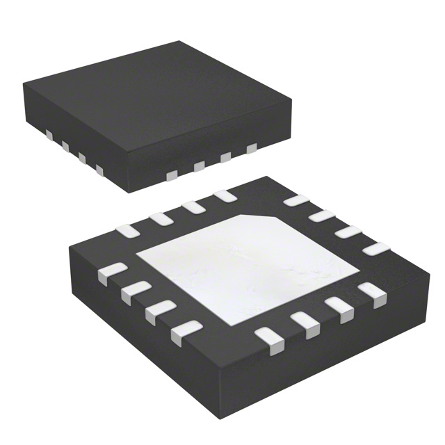
STMicroelectronics STEC01PUR
- Part No.:
- STEC01PUR
- Manufacturer:
- STMicroelectronics
- Category:
- Specialized ICs
- Package:
- 16-VFQFN Exposed Pad
- Datasheet:
-
 STEC01PUR.pdf
- Description:
- IC POWER SWITCH 16VFQFPN
- Quantity:
- Payment:

- Shipping:

Inventory:2,999
Please send an inquiry. Send us your inquiry, and we will respond immediately.
Product details
Overview
STEC01PUR from STMicroelectronics is a programmable low-side N-channel power switch IC with integrated 12 mΩ RDS(on) MOSFET, 7 A continuous current capability, and three independent timers (T1 up to 20480 s, T2 fixed at 285 ms, T3 at 69/345/1380 s) for ground-path safety control in high-current battery-powered actuators - deployed in electronic cigarettes to enforce user-defined heater on-time limits and thermal cooldown windows.
For engineers reviewing the STEC01PUR datasheet, STEC01PUR pinout, STEC01PUR application, or STEC01PUR equivalent, this device requires attention to PWM timing compliance (4 Hz–5 kHz, ≥30% duty cycle), T1/T3 resistor-programmed oscillator (TPF pin), HW_RESET debounced edge detection, and GDRV-driven external MOSFET support for >7 A loads.
Technical Context
The STEC01PUR implements a state-machine-based safety controller that monitors PWM activity to initiate T1 (programmable on-time), triggers T2 (285 ms fixed) upon PWM cessation to confirm end-of-cycle, and enforces T3 (user-selectable cooling window) after fault detection. It uses dual oscillator sources: one programmable via TPF resistor (100–400 kHz), one fixed for T2.
Its internal 12 mΩ N-channel MOSFET operates as a low-side switch between PWR (drain) and PGND (source), while GDRV provides gate drive for external N-MOSFETs. Fault response includes immediate SF turn-off, 57 ms open-drain RESET/FAULT pulse, and mandatory PWM low-level hold (>285 ms) before T3 initiation.
Key Specifications
| Parameter | Value and Actual Design Meaning |
|---|---|
| Input voltage range | 2.2 V to 5 V - supports single-cell Li-ion/Li-poly battery operation without external regulation. |
| RDS(on) | 12 mΩ typ. at VBAT = 2.5 V, IPWR = 1 A - enables ≤0.5 W conduction loss at 7 A, reducing thermal stress. |
| Continuous current | 7 A - maximum safe DC load current through internal MOSFET without external assistance. |
| PWM frequency range | 4 Hz to 5 kHz - defines valid control signal bandwidth for actuator modulation and timer synchronization. |
| Battery supply current | 30 µA active mode - ensures minimal drain during operational periods in portable devices. |
| Idle current | 2–4 µA typical, ≤10 µA over -40°C to +85°C - extends battery life during standby between actuation cycles. |
| T1 timer range | 5 s to 20480 s (≈5.7 h) - configurable via TPF resistor and T1P1/T1P2 prescaler selection per truth table. |
| T3 cooling window | 69 s / 345 s / 1380 s - selectable via T3P pin state to match thermal recovery requirements of heater elements. |
Pinout & Package
VFQFPN 3×3×0.9 mm, 16-lead, 0.5 mm pitch package with exposed thermal pad (GND EXP) for enhanced heat dissipation; RoHS-compliant ECOPACK2 grade.
| Pin/Terminal | Circuit Role | Design Meaning |
|---|---|---|
| RESET/FAULT (1) | Open-drain fault indicator output | Generates 57 ms active-low pulse on fault or HW_RESET event; requires external pull-up for MCU GPIO detection. |
| VBAT (2) | Battery supply input | Primary power rail; must be bypassed with 1 µF ceramic capacitor to AGND for stability. |
| AGND (3) | Analog ground reference | Dedicated low-noise ground path for timing circuitry and oscillator; separate from PGND. |
| TPF (4) | T1 oscillator programming input | Resistor-to-GND sets base oscillator frequency (100–400 kHz); directly scales T1 duration. |
| T1P1 (5), T1P2 (6) | T1 prescaler configuration inputs | Hard-wired logic pins selecting x1/x4/x16/x64 prescaler; determine T1 time resolution and range. |
| T3P (7) | T3 duration selection input | Hard-wired pin setting T3 to 69 s (floating), 345 s (0), or 1380 s (1); defines mandatory cooldown period. |
| PGND (8,9,10) | Power ground (MOSFET source) | High-current return path for internal FET; must be low-impedance connection to PCB ground plane. |
| PWR (11,12,13) | Power input (MOSFET drain) | Connects to battery-positive side of load; handles full 7 A current; multiple pins reduce resistance. |
| GDRV (14) | External MOSFET gate driver output | Drives N-channel gate for >7 A applications; left floating when internal FET suffices. |
| HW_RESET/USB (15) | Hardware reset input | Edge-triggered input (10 ms deglitch); rising edge signals external power connection (e.g., USB insertion). |
| PWM (16) | Control signal input | Accepts 4 Hz–5 kHz, 30–100% duty cycle pulses; rising edge initiates T1 and turns on SF. |
| GND EXP | Exposed thermal pad | Must be soldered to thermal ground plane; contributes to RthJC = 5 °C/W and RthJA = 42 °C/W. |
Key Features
| Feature | Design Value |
|---|---|
| Programmable on-time safety timer (T1) | Configurable from 5 s to 20480 s using TPF resistor and T1P1/T1P2 prescaler selection - enables precise actuator runtime enforcement. |
| Thermal-cooldown enforcement (T3) | Three discrete cooling windows (69/345/1380 s) selected by T3P pin - prevents premature reactivation after overtemperature or overtime fault. |
| Integrated low-RDS(on) power switch | 12 mΩ typ. N-channel MOSFET rated for 7 A continuous - eliminates need for external switch in sub-7 A e-cigarette heater applications. |
| External MOSFET drive capability | GDRV pin delivers sufficient gate drive to control external N-MOSFETs - extends current handling beyond 7 A with minimal BOM addition. |
| USB/VBUS presence detection | HW_RESET pin generates synchronized 57 ms RESET/FAULT pulse on rising edge - enables MCU-based charging-state notification without extra comparators. |
| Fault recovery protocol | Requires stable PWM low level (>285 ms) before T3 starts - prevents spurious restarts during transient noise or incomplete fault clearance. |
Applications
| Electronic Cigarette Heater Control | USB-Powered Device Safety Sequencing |
|---|---|
|
Use Scenario: Regulating power delivery to resistive heating coil in e-cigarette to prevent overheating and dry puff. IC Role / Device Role / Timing Role: Low-side safety switch enforcing user-configurable on-time (T1) and mandatory cooldown (T3) before next activation. Use Value: Eliminates risk of coil burnout or battery thermal runaway by cutting ground path precisely after programmed duration and enforcing thermal recovery. |
Use Scenario: Detecting USB cable insertion to trigger system wake-up and charging initialization in portable medical devices. IC Role / Device Role / Timing Role: Hardware reset interface translating VBUS rise into timed 57 ms pulse for MCU GPIO capture. Use Value: Provides deterministic, glitch-immune USB presence signal without software polling or external RC debounce circuits. |
| Inductive Actuator Protection | Portable Power Tool Thermal Management |
|
Use Scenario: Controlling solenoid or relay coil in handheld diagnostic tools where inductive kickback and dwell time must be managed. IC Role / Device Role / Timing Role: Ground-path switch with T2-based dwell validation and T1-based max-on-time limit to prevent coil saturation and thermal damage. Use Value: Prevents coil overheating by terminating power after validated PWM sequence ends or exceeding safe dwell threshold. |
Use Scenario: Managing motor driver enable path in cordless power tools to enforce duty-cycle limits and thermal cooldown between bursts. IC Role / Device Role / Timing Role: Programmable safety gate between battery and H-bridge, using T1 for burst duration and T3 for inter-burst cooling. Use Value: Extends tool runtime and battery life by preventing cumulative thermal stress across repeated high-current operations. |
Equivalent & Alternatives
The following parts are listed as comparable options for similar programmable low-side safety switch applications.
| Alternative Part | Technical Difference | Application Difference | Selection Advice |
|---|---|---|---|
| ON Semiconductor NCP380LSN35T2G | Fixed 3.5 mΩ RDS(on), no programmable timers; only overcurrent and overtemperature protection. | Lacks T1/T3 timing control - suitable for simple current-limiting but not for user-defined on-time or cooldown enforcement. | Select only if application requires only basic overcurrent cutoff without time-based safety sequencing. |
| Infineon BTS50085-1TAD | High-side switch with 8.5 mΩ RDS(on), integrated diagnostics, but no user-programmable timers or cooling window logic. | Designed for automotive load driving with SPI interface; lacks T3-style thermal cooldown enforcement and PWM-based activation. | Prefer for 12 V automotive systems needing diagnostic feedback, not for battery-powered consumer devices requiring programmable safety timing. |
Compared with NCP380LSN35T2G and BTS50085-1TAD, STEC01PUR uniquely integrates programmable multi-stage timing (T1/T2/T3) specifically for battery-powered thermal safety, enabling precise on-time enforcement and mandatory cooldown - features absent in fixed-protection or high-side automotive switches.
Availability
STEC01PUR is available at Aetrix Electronics and suitable for electronic cigarette manufacturing, USB-aware portable medical devices, inductive actuator control modules, and cordless power tool thermal management systems requiring stable component supply and long-term lifecycle support.
Supply support for STEC01PUR includes scheduled delivery planning, volume procurement assistance, BOM continuity management, traceable sourcing, and lifecycle availability coordination for OEM customers, industrial embedded developers, connected-device designers, and electronics production programs.
Manufacturer
STMicroelectronics is a global semiconductor leader headquartered in Geneva, Switzerland, designing and manufacturing microcontrollers, power management ICs, sensors, and analog components for industrial, automotive, and consumer markets.
STEC01PUR belongs to ST's dedicated safety power switch product line, engineered for battery-powered portable devices requiring programmable thermal and timing-based protection - especially where regulatory compliance (e.g., IEC 62368-1) mandates enforced cooldown intervals and user-actuated on-time limits.
FAQ
What is the minimum PWM pulse width required to reliably trigger the STEC01PUR?
The datasheet specifies a minimum PWM high time (tPWM_HI) of 40 µs. This ensures the internal logic detects the rising edge and initiates T1 before the pulse ends. Shorter pulses may fail to register, especially under temperature extremes or voltage variations, leading to inconsistent activation.
Can the STEC01PUR drive an external MOSFET for loads exceeding 7 A, and what are the GDRV voltage limits?
Yes - GDRV outputs a rail-to-rail signal referenced to PGND, with high-side resistance of 30 Ω and low-side resistance of 8 Ω. Its absolute maximum rating is VGBAT + 0.3 V, allowing direct drive of N-channel MOSFETs with VGS up to ~5.3 V when VBAT = 5 V. External gate resistors are recommended for EMI control and ringing suppression.
How does the STEC01PUR distinguish between normal PWM cessation and a fault condition?
It uses T2 (285 ms fixed timer): if PWM goes low and stays low longer than T2, the device enters idle mode normally. If PWM remains high past the programmed T1 duration, it triggers fault mode - turning off SF, asserting RESET/FAULT, and initiating T3 cooldown. T2 expiration alone does not cause fault; only T1 overrun does.
Is the TPF pin sensitive to PCB layout or capacitor loading, and what tolerance resistor is recommended?
Yes - TPF is a high-impedance oscillator programming node. Layout must minimize trace length and avoid nearby noisy signals or capacitive coupling. A 1% tolerance metal-film resistor is recommended; values from 91 kΩ to 400 kΩ set T1 within datasheet-specified min/max bounds, with tighter tolerance improving timer accuracy across temperature.
STEC01PUR Specifications
- Product attributes
- Attribute value
- Manufacturer:
- STMicroelectronics
- Series:
- -
- Package/Case:
- 16-VFQFN Exposed Pad
- Packaging:
- Tape & Reel (TR)
- Product Status:
- Active
- Programmable:
- Not Verified
- Type:
- Power Switch
- Applications:
- Protection Circuitry
- Mounting Type:
- Surface Mount
- Supplier Device Package:
- 16-VFQFPN (3x3)
- Grade:
- -
- Qualification:
- -
STEC01PUR FAQ
1.How can I place an order for STEC01PUR through Aetrix?
Please submit a Request for Quotation (RFQ) for STEC01PUR on Aetrix. Our sales agent will provide a competitive quotation and guide you through the order confirmation once you accept the terms.
2.Are the price and stock information for STEC01PUR reliable?
The price and inventory of STEC01PUR are updated periodically and may fluctuate due to market conditions. Stock and pricing data are typically refreshed every 24 hours. Quotation validity for STEC01PUR is usually 5 days.
3.What payment methods are accepted for STEC01PUR?
We accept Wire Transfer, PayPal, Credit Card, Western Union, MoneyGram, and Escrow for STEC01PUR transactions.
Note: Certain payment methods may incur a processing fee.
4.How is shipping managed for STEC01PUR?
STEC01PUR orders can be shipped via leading logistics carriers, including DHL, UPS, FedEx, TNT, or Registered Mail.
Once your STEC01PUR order is processed, you will receive an email with the shipment details and tracking number.
Note: Tracking information may take up to 24 hours to appear. Express delivery typically takes 3–5 business days.
5.How can I obtain technical support or documentation for STEC01PUR?
For technical support, including STEC01PUR datasheets, pinout diagrams, or application guidance, please contact our engineering support team. They can provide detailed documentation and assistance for your STEC01PUR requirements.
6.How does Aetrix verify that STEC01PUR is sourced from the original manufacturer or authorized distributors?
All STEC01PUR products on Aetrix are procured from qualified distributors and authorized channels. Our dedicated quality assurance team conducts strict verification, including traceability checks and, if necessary, third-party testing. This ensures that STEC01PUR meets industry standards.
7.What is the process for return or replacement of STEC01PUR?
All STEC01PUR units undergo pre-shipment inspection (PSI). If there is an issue with STEC01PUR, returns or replacements are accepted under the following conditions:
1.Quantity discrepancies, incorrect items, or visible external defects (such as breakage or corrosion), acknowledged by Aetrix.
2.The issue is reported within 90 days of delivery.
3.The STEC01PUR part is unused and in its original packaging.
Return procedure for STEC01PUR:
1.Submit a request within 90 days.
2.Obtain a Return Material Authorization (RMA) from Aetrix.
STEC01PUR Tags

-
CAP200DG-TL
Power Integrations
-
ATSHA204A-MAHDA-T
Microchip Technology

-
ATSHA204A-SSHDA-T
Microchip Technology

-
ATSHA204A-STUCZ-T
Microchip Technology
-
ATECC608B-MAHDA-T
Microchip Technology
-
ATECC608B-MAHCZ-S
Microchip Technology

-
ATECC608B-SSHDA-T
Microchip Technology
-
ATECC608B-MAHDA-S
Microchip Technology
-
ATECC608A-MAHDA-S
Microchip Technology
-
ATECC608B-MAVDA-T
Microchip Technology

-
ATECC608A-SSHDA-T
Microchip Technology
-
ATECC508A-MAHDA-T
Microchip Technology
Tech Hub

A practical engineering and sourcing framework covering lifecycle verification, lifetime-buy calculations, replacement qualification, supplier checks and counterfeit-risk controls.

TTL and CMOS logic families differ in thresholds, loading, output drive, power and timing. This engineering guide compares 74HC and 74HCT, calculates noise margins and checks 3.3 V/5 V compatibility.

A practical engineering guide to 3.3V and 5V logic compatibility, input thresholds, resistor dividers, translator ICs, MOSFET level shifting, I2C pull-ups, timing limits and power-sequencing risks.

The 74HC595 uses push-pull logic outputs, while the TPIC6B595 uses 50 V open-drain DMOS sinks for higher-power loads. This guide compares timing, current limits, 3.3 V interfacing, load wiring, thermal…

The 74HC595 converts serial data into eight stable parallel outputs. This guide covers pin functions, shift and storage timing, OE and MR behavior, drive-current limits, cascading, voltage compatibilit…

A technical comparison of level-sensitive latches and edge-triggered flip-flops, covering timing windows, setup and hold limits, master–slave operation, time borrowing, race-through, HDL inference and…

A D latch stores one bit while Enable controls when data can pass. This reference covers gate-level operation, truth tables, transparency, setup and hold timing, LE versus OE, common ICs and practical …

An SR latch stores one bit through cross-coupled feedback. This engineering reference covers NOR and NAND implementations, truth tables, forbidden-state recovery, gated operation, switch debouncing, fa…

Latch circuits retain one bit through feedback. This technical reference covers SR and D latches, truth tables, transparency, timing limits, latch-versus-flip-flop behavior, applications and common log…

An engineering guide to LED driver operation, constant-current and constant-voltage outputs, linear and switching topologies, dimming, IC selection, calculations, replacement compatibility, and fault c…


