
 My Inquiry
 My Account


STMicroelectronics STEF05LAJR
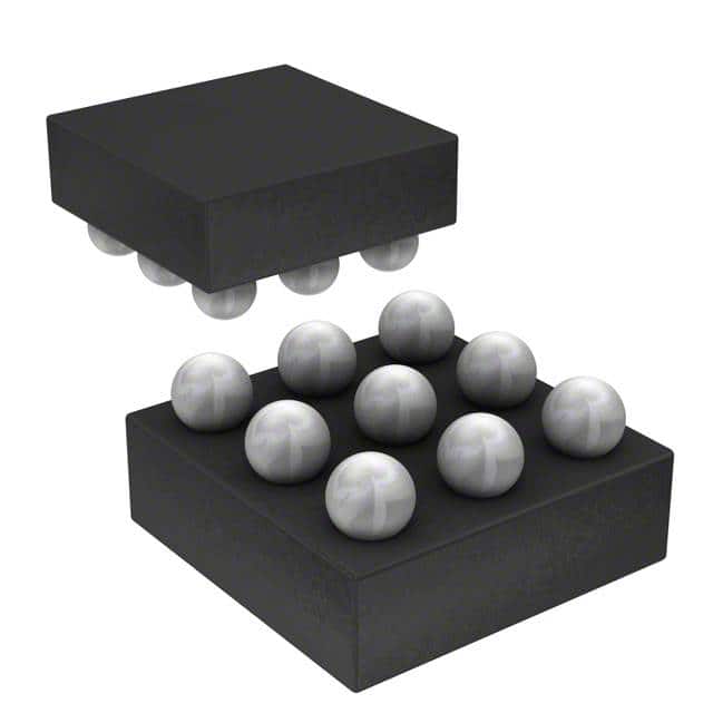
- Part No.:
- STEF05LAJR
- Manufacturer:
- STMicroelectronics
- Category:
- Current Regulation/Management
- Package:
- 9-UFBGA, FCBGA
- Datasheet:
-
 STEF05LAJR.pdf
- Description:
- IC ELECTRONIC FUSE 9FLIPCHIP
- Quantity:
- Payment:

- Shipping:

Inventory:3,750
Please send an inquiry. Send us your inquiry, and we will respond immediately.
Product details
Overview
STEF05LAJR from STMicroelectronics is a latching electronic fuse (eFuse) optimized for 5 V rail protection in high-reliability storage systems. It integrates an N-channel power MOSFET with 25 mΩ typical RDS(on) (Flip Chip package), 2.5 A continuous current rating, 6.1 V output clamping voltage, and thermal latch at 160 °C. It operates across –40 °C to 125 °C junction temperature and supports controlled soft-start via internal dv/dt circuitry - used in SSDs and HDD arrays for overcurrent, overvoltage, and thermal fault protection.
For engineers reviewing the STEF05LAJR datasheet, STEF05LAJR pinout, STEF05LAJR application, or STEF05LAJR equivalent, this device requires attention to its dual-function Enable/Fault pin behavior, external current-limit resistor (RLimit) selection, Flip Chip 9-bump package layout constraints, and distinction between latching vs. auto-retry versions when designing fault-tolerant 5 V power distribution.
Technical Context
The STEF05LAJR implements a precision current-sense architecture using an internal N-Channel Sense FET with fixed ratio to monitor load current and enforce two-tiered limiting: overload trip-point (ILim = 2.5 A) and short-circuit clamp (IShort ≈ 1.5 A typ. with 24 Ω RLimit). Its voltage clamp circuit actively limits VOUT to ≤6.8 V under overvoltage conditions (e.g., input surge to 8 V).
Thermal protection uses a non-degrading latch mechanism triggered at 160 °C, signaled via intermediate voltage (0.8–2.0 V) on the bi-directional Enable/Fault pin. The device features programmable turn-on slew rate (1.4 ms baseline, extendable to 16 ms with external Cdv/dt) and undervoltage lockout (3.1–4.0 V turn-on threshold with 0.1 V hysteresis).
Key Specifications
| Parameter | Value and Actual Design Meaning |
|---|---|
| VIN Range | 4.5 V to 8 V - supports nominal 5 V rail with margin for transient overshoot and brownout resilience. |
| RDS(on) | 25 mΩ typ. - minimizes power loss (≤156 mW at 2.5 A) and self-heating in Flip Chip package. |
| ICONT | 2.5 A continuous - defines maximum steady-state load current before thermal derating applies. |
| VCLAMP | 6.1 V typ. - clamps output during input overvoltage (e.g., 8 V supply), protecting downstream 5 V logic. |
| TSD | 160 °C typ. - thermal latch point; prevents permanent damage during sustained overload or poor PCB heat sinking. |
| tDELAY | 500 µs - fixed delay from enable assertion to VOUT ramp initiation, aiding sequencing in multi-rail systems. |
| UVLO Threshold | 3.4 V typ. - ensures stable operation only above minimum functional voltage; 0.1 V hysteresis prevents chatter. |
Pinout & Package
STEF05LAJR is supplied in Flip Chip 9-bump package (1.19 mm × 1.19 mm, 0.55 mm height), optimized for ultra-compact SSD and HDD controller board layouts. Exposed die attach area provides low thermal resistance (RthJC not specified; RthJA = 90 °C/W).
| Pin/Terminal | Circuit Role | Design Meaning |
|---|---|---|
| VCC (B1–B3) | Positive input voltage terminal | Connects directly to 5 V rail; must be decoupled with ≥10 µF ceramic capacitor near package. |
| VOUT/Source (A1–A3) | Output/source node of internal MOSFET | Delivers protected 5 V to load; Kelvin sensing recommended for accurate current limit calibration. |
| I-Lim+ (A2) | Current limit reference input | Paired with Source pin via external resistor (15–120 Ω) to set IShort and ILim thresholds. |
| En/Fault (A2) | Tri-state bi-directional control/status pin | Float = enabled; pulled low = disable; intermediate voltage (0.8–2.0 V) = thermal fault signal. |
| GND (A3) | Ground reference | Low-impedance return path; must be connected to solid ground plane beneath exposed die pad. |
Key Features
| Feature | Design Value |
|---|---|
| Controlled output voltage ramp | 1.4 ms default VOUT rise time (10–90 %); adjustable up to 16 ms with external Cdv/dt - prevents inrush current in hot-plug SSD modules. |
| Output voltage clamping | Clamps VOUT to ≤6.8 V during input overvoltage - protects 5 V tolerant ICs (e.g., SATA PHY, NAND controller) without external TVS. |
| Latching thermal shutdown | Non-degrading 160 °C thermal latch with fault signaling - eliminates need for manual fuse replacement in inaccessible storage enclosures. |
| Enable/Fault dual functionality | Single-pin interface enables remote disable and receives thermal fault indication - reduces BOM count and routing complexity. |
| Kelvin current sensing support | Dedicated I-Lim+ and Source pins enable 4-wire sensing - maintains ±10 % current limit accuracy despite PCB trace resistance. |
Applications
| Solid State Drive (SSD) Power Management | Hard Disk Drive (HDD) Actuator Protection |
|---|---|
|
Use Scenario: Protecting NAND flash controller and DRAM buffer rails in M.2 and U.2 SSDs against short circuits during hot insertion or component failure. IC Role / Device Role / Timing Role: Series eFuse providing overcurrent and overvoltage isolation on the 5 V VCC rail, with <1.6 ms total turn-on delay including 500 µs internal delay and 1.4 ms dv/dt ramp. Use Value: Prevents catastrophic bus collapse during NAND channel shorts, enabling graceful firmware recovery instead of system-wide power loss. |
Use Scenario: Safeguarding voice coil motor (VCM) driver and preamp circuits in 2.5" enterprise HDDs subjected to mechanical shock-induced shorts. IC Role / Device Role / Timing Role: High-speed current limiter responding within microseconds to ISHORT events, with thermal latch preventing MOSFET destruction during sustained overload. Use Value: Maintains drive operability after transient faults by isolating damaged actuator circuitry while preserving spindle and servo subsystems. |
| HDD/SSD Array Backplane Protection | DVD/Blu-ray Optical Drive Power Distribution |
|
Use Scenario: Individual rail protection per drive slot in JBOD or RAID enclosures where shared 5 V supplies risk cascading failure. IC Role / Device Role / Timing Role: Independent eFuse per slot with Enable/Fault pin daisy-chained to central monitoring MCU for coordinated shutdown on thermal event. Use Value: Enables selective slot deactivation without powering down entire array - critical for hot-swap maintenance and serviceability. |
Use Scenario: Isolating laser diode driver and spindle motor circuits in consumer optical drives prone to ESD-induced latch-up. IC Role / Device Role / Timing Role: Fast-acting 5 V rail protector with 6.1 V clamping to suppress ESD transients on power inputs before they reach sensitive analog front-ends. Use Value: Eliminates need for discrete TVS + fuse combinations, reducing footprint by >40 % while improving response consistency. |
Equivalent & Alternatives
The following parts are listed as comparable options for similar electronic fuse applications.
| Alternative Part | Technical Difference | Application Difference | Selection Advice |
|---|---|---|---|
| TPS259211DRCT | 4.5–13.2 V input range; 3.5 A continuous; integrated 12-bit current monitor; no voltage clamping. | Requires external clamping for overvoltage; better suited for telemetry-rich industrial power rails than compact storage boards. | Choose if current measurement accuracy and wide VIN are prioritized over space-constrained layout and built-in clamping. |
| AP22653WMX-7 | 5.5 V max input; 2.2 A continuous; 45 mΩ RDS(on); no thermal latch or dv/dt control. | Lacks thermal fault signaling and programmable soft-start - insufficient for mission-critical SSD/HDD thermal management. | Select only for cost-sensitive, low-power peripherals where thermal robustness and precise ramp control are non-critical. |
Compared with TPS259211DRCT and AP22653WMX-7, STEF05LAJR uniquely combines Flip Chip miniaturization, integrated 6.1 V clamping, thermal latch with status signaling, and Kelvin-sensing compatibility - making it the only option qualified for high-density, thermally constrained storage power domains.
Availability
STEF05LAJR is available at Aetrix Electronics and suitable for solid state drives, hard disk drive arrays, and optical disc drive power distribution requiring stable component supply, long-term lifecycle support, and consistent Flip Chip 9-bump packaging.
Supply support for STEF05LAJR includes scheduled delivery planning, volume procurement assistance, BOM continuity management, traceable sourcing, and lifecycle availability coordination for OEM customers, industrial embedded developers, connected-device designers, and electronics production programs.
Manufacturer
STMicroelectronics is a global semiconductor leader headquartered in Geneva, Switzerland, specializing in power management, microcontrollers, and automotive-grade analog ICs.
STEF05LAJR belongs to ST's eFuse portfolio designed specifically for high-reliability 5 V power rail protection in data storage systems - emphasizing thermal robustness, compact packaging, and seamless integration with HDD/SSD controller architectures.
FAQ
What is the function of the En/Fault pin on STEF05LAJR?
The En/Fault pin serves dual roles: when left floating or pulled high, it enables the eFuse output; when pulled low (<0.5 V), it disables the output. During thermal shutdown, it transitions to an intermediate voltage (0.8–2.0 V) to signal fault condition to host monitoring circuitry - enabling coordinated shutdown across multiple devices when daisy-chained.
How is current limiting set on STEF05LAJR?
Current limiting is configured externally using a resistor (RLimit) between the I-Lim+ pin and the Source (VOUT) terminal. For STEF05LAJR, RLimit ranges from 15 Ω to 120 Ω, setting short-circuit current (IShort) between ~1.1 A and 1.9 A, and overload trip-point (ILim) at 2.5 A - values confirmed in Table 6 of DS11527 Rev 2.
Does STEF05LAJR support soft-start adjustment?
No - the STEF05LAJR (Flip Chip version) does not support external dv/dt capacitor adjustment. Unlike the DFN10 variant, its dv/dt circuit is internal-only with fixed 1.4 ms VOUT ramp time (10–90 %). The "dv/dt" pin is not present in the Flip Chip 9-bump configuration per Figure 2 and Table 1 of DS11527 Rev 2.
What is the difference between STEF05LJR and STEF05LAJR?
STEF05LJR is the latching version; STEF05LAJR is the auto-retry version. Both share identical electrical specs and package, but STEF05LAJR automatically attempts re-enabling after thermal fault when die temperature falls below hysteresis (≈135 °C), whereas STEF05LJR remains latched until supply cycling or active EN pin reset - critical for fail-safe vs. self-recovering system requirements.
STEF05LAJR Specifications
- Product attributes
- Attribute value
- Manufacturer:
- STMicroelectronics
- Series:
- -
- Package/Case:
- 9-UFBGA, FCBGA
- Packaging:
- Tape & Reel (TR)
- Product Status:
- Active
- Function:
- Electronic Fuse
- Sensing Method:
- -
- Accuracy:
- -
- Voltage - Input:
- 4.5V ~ 8V
- Current - Output:
- 2.5A
- Operating Temperature:
- -40°C ~ 125°C (TJ)
- Grade:
- -
- Qualification:
- -
- Mounting Type:
- Surface Mount
- Supplier Device Package:
- 9-FlipChip (1.19x1.19)
STEF05LAJR FAQ
1.How can I place an order for STEF05LAJR through Aetrix?
Please submit a Request for Quotation (RFQ) for STEF05LAJR on Aetrix. Our sales agent will provide a competitive quotation and guide you through the order confirmation once you accept the terms.
2.Are the price and stock information for STEF05LAJR reliable?
The price and inventory of STEF05LAJR are updated periodically and may fluctuate due to market conditions. Stock and pricing data are typically refreshed every 24 hours. Quotation validity for STEF05LAJR is usually 5 days.
3.What payment methods are accepted for STEF05LAJR?
We accept Wire Transfer, PayPal, Credit Card, Western Union, MoneyGram, and Escrow for STEF05LAJR transactions.
Note: Certain payment methods may incur a processing fee.
4.How is shipping managed for STEF05LAJR?
STEF05LAJR orders can be shipped via leading logistics carriers, including DHL, UPS, FedEx, TNT, or Registered Mail.
Once your STEF05LAJR order is processed, you will receive an email with the shipment details and tracking number.
Note: Tracking information may take up to 24 hours to appear. Express delivery typically takes 3–5 business days.
5.How can I obtain technical support or documentation for STEF05LAJR?
For technical support, including STEF05LAJR datasheets, pinout diagrams, or application guidance, please contact our engineering support team. They can provide detailed documentation and assistance for your STEF05LAJR requirements.
6.How does Aetrix verify that STEF05LAJR is sourced from the original manufacturer or authorized distributors?
All STEF05LAJR products on Aetrix are procured from qualified distributors and authorized channels. Our dedicated quality assurance team conducts strict verification, including traceability checks and, if necessary, third-party testing. This ensures that STEF05LAJR meets industry standards.
7.What is the process for return or replacement of STEF05LAJR?
All STEF05LAJR units undergo pre-shipment inspection (PSI). If there is an issue with STEF05LAJR, returns or replacements are accepted under the following conditions:
1.Quantity discrepancies, incorrect items, or visible external defects (such as breakage or corrosion), acknowledged by Aetrix.
2.The issue is reported within 90 days of delivery.
3.The STEF05LAJR part is unused and in its original packaging.
Return procedure for STEF05LAJR:
1.Submit a request within 90 days.
2.Obtain a Return Material Authorization (RMA) from Aetrix.
STEF05LAJR Tags
.jpg)
-
PSSI2021SAY,115
Nexperia USA Inc.

-
BCR401RE6327HTSA1
Infineon Technologies

-
INA199B2DCKR
Texas Instruments
-
INA199A1DCKR
Texas Instruments
-
INA199B1DCKR
Texas Instruments
-
NSI45015WT1G
onsemi
-
NSI45020T1G
onsemi
-
NSI45030AT1G
onsemi
-
NSI45025AT1G
onsemi
-
NSI45020AT1G
onsemi
-
NSI50010YT1G
onsemi
-
LM334Z/NOPB
Texas Instruments
Tech Hub

A practical engineering and sourcing framework covering lifecycle verification, lifetime-buy calculations, replacement qualification, supplier checks and counterfeit-risk controls.

TTL and CMOS logic families differ in thresholds, loading, output drive, power and timing. This engineering guide compares 74HC and 74HCT, calculates noise margins and checks 3.3 V/5 V compatibility.

A practical engineering guide to 3.3V and 5V logic compatibility, input thresholds, resistor dividers, translator ICs, MOSFET level shifting, I2C pull-ups, timing limits and power-sequencing risks.

The 74HC595 uses push-pull logic outputs, while the TPIC6B595 uses 50 V open-drain DMOS sinks for higher-power loads. This guide compares timing, current limits, 3.3 V interfacing, load wiring, thermal…

The 74HC595 converts serial data into eight stable parallel outputs. This guide covers pin functions, shift and storage timing, OE and MR behavior, drive-current limits, cascading, voltage compatibilit…

A technical comparison of level-sensitive latches and edge-triggered flip-flops, covering timing windows, setup and hold limits, master–slave operation, time borrowing, race-through, HDL inference and…

A D latch stores one bit while Enable controls when data can pass. This reference covers gate-level operation, truth tables, transparency, setup and hold timing, LE versus OE, common ICs and practical …

An SR latch stores one bit through cross-coupled feedback. This engineering reference covers NOR and NAND implementations, truth tables, forbidden-state recovery, gated operation, switch debouncing, fa…

Latch circuits retain one bit through feedback. This technical reference covers SR and D latches, truth tables, transparency, timing limits, latch-versus-flip-flop behavior, applications and common log…

An engineering guide to LED driver operation, constant-current and constant-voltage outputs, linear and switching topologies, dimming, IC selection, calculations, replacement compatibility, and fault c…


