
 My Inquiry
 My Account


STMicroelectronics STG3696EQTR
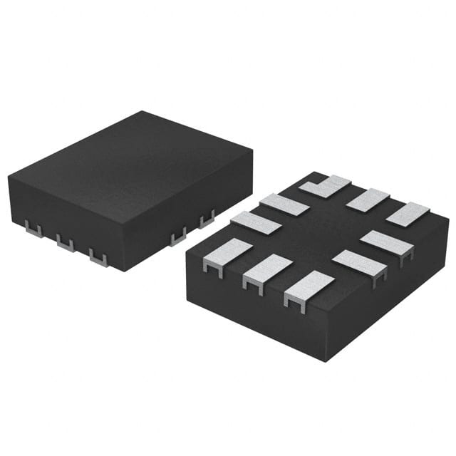
- Part No.:
- STG3696EQTR
- Manufacturer:
- STMicroelectronics
- Category:
- Analog Switches - Special Purpose
- Package:
- 10-UFQFN
- Datasheet:
-
 STG3696EQTR.pdf
- Description:
- IC SWITCH SPDT USB/AUDIO 10-QFN
- Quantity:
- Payment:

- Shipping:

Inventory:4,811
Please send an inquiry. Send us your inquiry, and we will respond immediately.
Product details
Overview
STG3696EQTR from STMicroelectronics is a low-voltage dual SPDT analog switch optimized for concurrent USB 2.0 high-speed (480 Mbps) and bidirectional audio signal routing in mobile devices. It features 2.5 Ω typical RON, ±8 kV HBM ESD protection on COM pins, 950 MHz –3 dB bandwidth, auto VBUS detection for seamless mode switching, and negative-swing audio capability down to VCC – 5.0 V - enabling ground-referenced headphone amplifiers without external charge pumps.
For engineers reviewing the STG3696EQTR datasheet, STG3696EQTR pinout, STG3696EQTR application, or STG3696EQTR equivalent, this device addresses critical coexistence challenges between high-speed digital and high-fidelity analog paths in space-constrained portable designs - particularly where pop-noise suppression, fault tolerance to 5.5 V overvoltage, and channel-to-channel crosstalk below –70 dB are mandatory.
Technical Context
The STG3696E integrates two independent SPDT switches sharing common COM1/COM2 terminals, each configurable via VBUS voltage sensing or AOVR override control. Its internal negative charge pump enables true rail-to-rail audio signal handling including sub-ground excursions, while dedicated shunt resistors (200 Ω) discharge floating AUn lines to suppress pop/click noise during switching transitions.
Fault protection activates when COMn voltage exceeds VOVDT (VCC + 0.35 V), disconnecting channels within 1.3 µs and recovering in under 55 µs. USB path maintains <8 pF on-capacitance and <5 Ω RON matching (±0.5 Ω), meeting USB 2.0 eye diagram integrity requirements at 480 Mbps.
Key Specifications
| Parameter | Value and Actual Design Meaning |
|---|---|
| VCC Range | 2.7 V to 4.5 V - supports single-supply operation from Li-ion battery or LDO rails without level-shifting. |
| RON (Audio) | 2.4 Ω typ. - ensures minimal insertion loss and THD+N < 0.05% across 20 Hz–20 kHz audio band. |
| RON (USB) | 2.4 Ω typ. - preserves signal integrity for USB 2.0 differential pairs with <0.5 Ω matching between channels. |
| Bandwidth (–3 dB) | 950 MHz - accommodates full USB 2.0 spectral content and harmonics without attenuation. |
| ESD Protection | ±8 kV HBM on COM pins - eliminates need for external TVS diodes in handheld ESD-prone interfaces. |
| Crosstalk | –70 dB @ 100 kHz - prevents audible leakage between left/right audio channels or USB/data coupling. |
| Pop Noise Suppression | Integrated 200 Ω shunt resistors - actively discharge AUn nodes during idle state to eliminate transient transients. |
Pinout & Package
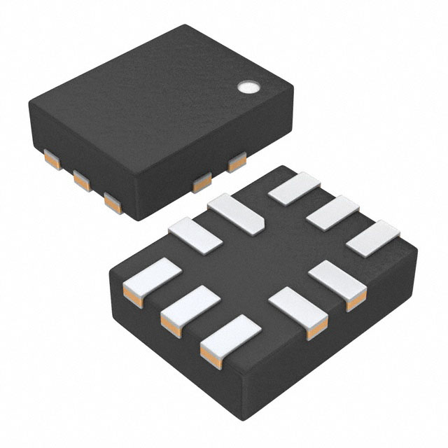
STG3696EQTR uses a 10-pin QFN package (1.8 mm × 1.4 mm × 0.5 mm, 0.4 mm pitch) with wettable flanks and exposed thermal pad. Pin 1 is marked by a dot at top-left corner (TLC).
| Pin/Terminal | Circuit Role | Design Meaning |
|---|---|---|
| 1 (USB1) | USB data channel 1 input | Connects to D+ or D– of upstream USB transceiver; withstands 5.5 V fault events. |
| 2 (AU2) | Audio channel 2 input | Supports negative swing to VCC – 5.0 V; internally shunted when unselected. |
| 3 (AU1) | Audio channel 1 input | Primary left/right audio path; identical electrical behavior to AU2. |
| 4 (GND) | Digital/analog reference ground | Common return for all signals; must be connected to low-impedance PCB ground plane. |
| 5 (VCC) | Positive supply | Powers internal charge pump, logic, and switch arrays; bypass capacitor required. |
| 6 (COM1) | Common output 1 | Shared node for USB1/AU1 selection; connects to connector or codec interface. |
| 7 (COM2) | Common output 2 | Shared node for USB2/AU2 selection; electrically isolated from COM1. |
| 8 (AOVR) | Audio override enable | High = force audio path; low = enable automatic VBUS-triggered switching. |
| 9 (VBUS) | USB power detection input | Threshold at 0.5×VCC; triggers reconfiguration without external comparator. |
| 10 (USB2) | USB data channel 2 input | Second USB differential line; matched impedance and timing to USB1. |
Key Features
| Feature | Design Value |
|---|---|
| Auto VBUS detection | Eliminates external voltage monitor IC and reduces BOM count in dual-mode USB/audio accessories. |
| Negative rail audio support | Enables direct connection to Class AB headphone amplifiers without external negative supply generation. |
| Integrated pop-noise shunts | 200 Ω internal resistors discharge floating audio inputs, removing need for discrete RC networks. |
| USB 2.0 fault protection | Withstands 5.5 V overvoltage on COM pins per USB specification, protecting downstream PHYs. |
| Low RON flatness | 0.03 Ω (audio), 0.05 Ω (USB) - ensures consistent gain and impedance across full signal swing range. |
Applications
| Smartphone Audio/USB Switching | USB-C Docking Adapter |
|---|---|
Use Scenario: Simultaneous headphone playback and USB data transfer in compact smartphones using shared physical connector. IC Role / Device Role / Timing Role: Dual SPDT switch dynamically routes COM1/COM2 between AU1/AU2 and USB1/USB2 based on VBUS presence. Use Value: Enables single USB-C port to serve as both audio jack and data interface without mechanical switching or user intervention. | Use Scenario: Multi-function docking station supporting audio output, USB 2.0 peripherals, and charging through one upstream port. IC Role / Device Role / Timing Role: Isolates audio DAC outputs from USB data lines while maintaining signal integrity during hot-plug events. Use Value: Prevents USB packet corruption and audio artifacts during concurrent use, validated at 480 Mbps with <8 pF CON. |
| Portable Media Player | USB OTG Audio Interface |
Use Scenario: MP3 player with integrated line-out and USB mass storage mode sharing same micro-USB connector. IC Role / Device Role / Timing Role: Switches analog audio path to 3.5 mm jack when no VBUS detected; reconfigures to USB data path upon host connection. Use Value: Achieves zero-pop switching with <5 µs tOFF and <85 µs tON, eliminating audible clicks during mode transition. | Use Scenario: Android OTG accessory that adds stereo audio input/output while retaining USB host functionality. IC Role / Device Role / Timing Role: Routes microphone/line-in signals to codec while allowing simultaneous USB enumeration and HID communication. Use Value: Maintains <–65 dB off-isolation to prevent USB noise coupling into sensitive analog input paths. |
Equivalent & Alternatives
The following parts are listed as comparable options for similar dual SPDT USB/audio switching applications.
| Alternative Part | Technical Difference | Application Difference | Selection Advice |
|---|---|---|---|
| TS5USBA225RSER | No integrated negative charge pump; audio swing limited to GND–VCC; lower ESD (±4 kV HBM). | Requires external biasing for true ground-referenced audio; unsuitable for sub-ground headphone drivers. | Select only if system uses AC-coupled audio or has external negative rail. |
| MAX4989ETE+ | Higher RON (4.5 Ω typ.), no VBUS auto-detect; requires GPIO-controlled mode selection. | Needs additional MCU pin and firmware logic for USB/audio arbitration; larger 16-pin TQFN package. | Choose when precise timing control over switching sequence is required over automatic detection. |
Compared with TS5USBA225RSER and MAX4989ETE+, STG3696EQTR uniquely combines VBUS-triggered auto-switching, integrated negative rail generation, and ±8 kV ESD in a 10-pin QFN - reducing component count and PCB area while enabling robust dual-mode operation without software intervention.
Availability
STG3696EQTR is available at Aetrix Electronics and suitable for smartphone audio routing, USB-C docking adapters, and portable media players requiring stable component supply, long-term lifecycle support, and RoHS-compliant packaging.
Supply support for STG3696EQTR includes scheduled delivery planning, volume procurement assistance, BOM continuity management, traceable sourcing, and lifecycle availability coordination for OEM customers, industrial embedded developers, connected-device designers, and electronics production programs.
Manufacturer
STMicroelectronics is a global semiconductor leader headquartered in Geneva, Switzerland, designing and manufacturing microcontrollers, power management ICs, sensors, and analog switches for industrial, automotive, and consumer markets.
The STG3696E belongs to ST's high-performance analog switch portfolio targeting mobile connectivity, where low RON, ultra-low capacitance, and integrated protection features address stringent size, power, and reliability requirements of handheld USB/audio interfaces.
FAQ
What is the maximum allowable voltage on the COM pins during overvoltage fault conditions?
The COM pins tolerate up to 5.5 V in overvoltage fault conditions per USB 2.0 specification. When voltage exceeds VOVDT (VCC + 0.35 V), the internal protection circuit disconnects the channel within 1.3 µs to safeguard downstream components like USB transceivers or audio codecs.
How does the internal negative charge pump operate, and what are its limitations?
The integrated negative charge pump generates a local negative rail enabling audio signals to swing down to VCC – 5.0 V on AU1/AU2 pins. It operates automatically when audio path is selected and AOVR is high or VBUS is absent. The pump is disabled during USB mode to avoid interference; applying negative voltage to AUn pins during fault protection activation may damage the device.
Can STG3696EQTR be used in systems without VBUS detection capability?
Yes - driving AOVR high forces permanent audio path selection regardless of VBUS state. This allows manual control in systems lacking VBUS monitoring, such as legacy USB-A docks or standalone audio accessories. In this mode, USB1/USB2 pins remain inactive but retain full 5.5 V fault tolerance.
What layout guidelines are critical for maintaining 950 MHz bandwidth and low crosstalk?
Route COM1/COM2 traces differentially with controlled 50 Ω impedance; separate USB and audio paths with ground guard traces; place 100 nF VCC bypass capacitor within 2 mm of pin 5; connect exposed thermal pad to solid ground plane using ≥4 thermal vias; avoid stubs longer than 1 mm on any high-speed line.
STG3696EQTR Specifications
- Product attributes
- Attribute value
- Manufacturer:
- STMicroelectronics
- Series:
- -
- Package/Case:
- 10-UFQFN
- Packaging:
- Tape & Reel (TR)
- Product Status:
- Active
- Applications:
- Audio, USB
- Multiplexer/Demultiplexer Circuit:
- 2:1
- Switch Circuit:
- SPDT
- Number of Channels:
- 2
- On-State Resistance (Max):
- 5Ohm
- Voltage - Supply, Single (V+):
- 2.7V ~ 4.5V
- Voltage - Supply, Dual (V±):
- -
- -3db Bandwidth:
- 850MHz
- Features:
- USB 2.0
- Operating Temperature:
- -40°C ~ 85°C (TA)
- Grade:
- -
- Qualification:
- -
- Mounting Type:
- Surface Mount
- Supplier Device Package:
- 10-QFN (1.8x1.4)
STG3696EQTR FAQ
1.How can I place an order for STG3696EQTR through Aetrix?
Please submit a Request for Quotation (RFQ) for STG3696EQTR on Aetrix. Our sales agent will provide a competitive quotation and guide you through the order confirmation once you accept the terms.
2.Are the price and stock information for STG3696EQTR reliable?
The price and inventory of STG3696EQTR are updated periodically and may fluctuate due to market conditions. Stock and pricing data are typically refreshed every 24 hours. Quotation validity for STG3696EQTR is usually 5 days.
3.What payment methods are accepted for STG3696EQTR?
We accept Wire Transfer, PayPal, Credit Card, Western Union, MoneyGram, and Escrow for STG3696EQTR transactions.
Note: Certain payment methods may incur a processing fee.
4.How is shipping managed for STG3696EQTR?
STG3696EQTR orders can be shipped via leading logistics carriers, including DHL, UPS, FedEx, TNT, or Registered Mail.
Once your STG3696EQTR order is processed, you will receive an email with the shipment details and tracking number.
Note: Tracking information may take up to 24 hours to appear. Express delivery typically takes 3–5 business days.
5.How can I obtain technical support or documentation for STG3696EQTR?
For technical support, including STG3696EQTR datasheets, pinout diagrams, or application guidance, please contact our engineering support team. They can provide detailed documentation and assistance for your STG3696EQTR requirements.
6.How does Aetrix verify that STG3696EQTR is sourced from the original manufacturer or authorized distributors?
All STG3696EQTR products on Aetrix are procured from qualified distributors and authorized channels. Our dedicated quality assurance team conducts strict verification, including traceability checks and, if necessary, third-party testing. This ensures that STG3696EQTR meets industry standards.
7.What is the process for return or replacement of STG3696EQTR?
All STG3696EQTR units undergo pre-shipment inspection (PSI). If there is an issue with STG3696EQTR, returns or replacements are accepted under the following conditions:
1.Quantity discrepancies, incorrect items, or visible external defects (such as breakage or corrosion), acknowledged by Aetrix.
2.The issue is reported within 90 days of delivery.
3.The STG3696EQTR part is unused and in its original packaging.
Return procedure for STG3696EQTR:
1.Submit a request within 90 days.
2.Obtain a Return Material Authorization (RMA) from Aetrix.
STG3696EQTR Tags
-
TS3USB221ARSER
Texas Instruments
-
TS3USB221AQRSERQ1
Texas Instruments
-
NX3DV221GM,115
NXP Semiconductors
-
NX3DV2567GU,115
NXP Semiconductors
-
TS3USB221RSER
Texas Instruments
-
TS3USB221ERSER
Texas Instruments
-
TC7USB40MU,LF(S2E
Toshiba Semiconductor and Storage

-
TS3USB30EDGSR
Texas Instruments
-
PI3USB221AZUAEX
Diodes Incorporated
-
FSUSB42UMX
onsemi
-
CBTL01023GM,115
NXP Semiconductors
-
TS3USB30ERSWR
Texas Instruments
Tech Hub

A practical engineering and sourcing framework covering lifecycle verification, lifetime-buy calculations, replacement qualification, supplier checks and counterfeit-risk controls.

TTL and CMOS logic families differ in thresholds, loading, output drive, power and timing. This engineering guide compares 74HC and 74HCT, calculates noise margins and checks 3.3 V/5 V compatibility.

A practical engineering guide to 3.3V and 5V logic compatibility, input thresholds, resistor dividers, translator ICs, MOSFET level shifting, I2C pull-ups, timing limits and power-sequencing risks.

The 74HC595 uses push-pull logic outputs, while the TPIC6B595 uses 50 V open-drain DMOS sinks for higher-power loads. This guide compares timing, current limits, 3.3 V interfacing, load wiring, thermal…

The 74HC595 converts serial data into eight stable parallel outputs. This guide covers pin functions, shift and storage timing, OE and MR behavior, drive-current limits, cascading, voltage compatibilit…

A technical comparison of level-sensitive latches and edge-triggered flip-flops, covering timing windows, setup and hold limits, master–slave operation, time borrowing, race-through, HDL inference and…

A D latch stores one bit while Enable controls when data can pass. This reference covers gate-level operation, truth tables, transparency, setup and hold timing, LE versus OE, common ICs and practical …

An SR latch stores one bit through cross-coupled feedback. This engineering reference covers NOR and NAND implementations, truth tables, forbidden-state recovery, gated operation, switch debouncing, fa…

Latch circuits retain one bit through feedback. This technical reference covers SR and D latches, truth tables, transparency, timing limits, latch-versus-flip-flop behavior, applications and common log…

An engineering guide to LED driver operation, constant-current and constant-voltage outputs, linear and switching topologies, dimming, IC selection, calculations, replacement compatibility, and fault c…


