
 My Inquiry
 My Account


STMicroelectronics STM3240G-SK/KEI
- Part No.:
- STM3240G-SK/KEI
- Manufacturer:
- STMicroelectronics
- Category:
- Embedded MCU, DSP Evaluation Boards
- Package:
- Datasheet:
-
 STM3240G-SK/KEI.pdf
- Description:
- STM32F407 EVAL BRD
- Quantity:
- Payment:

- Shipping:

Inventory:3,140
Please send an inquiry. Send us your inquiry, and we will respond immediately.
Product details
Overview
STM32F407VG from STMicroelectronics is a 32-bit Arm® Cortex®-M4 MCU with FPU, operating up to 168 MHz, featuring 1 MB flash, 192+4 KB SRAM (including 64 KB CCM), dual CAN 2.0B interfaces, 10/100 Ethernet MAC with IEEE 1588v2 hardware support, and USB OTG HS/FS controllers - deployed in industrial gateway controllers requiring real-time protocol bridging and deterministic network timing.
For engineers reviewing the STM32F407VG datasheet, STM32F407VG pinout, STM32F407VG application, or STM32F407VG equivalent, key selection criteria include Ethernet MAC timing compliance, dual-CAN arbitration latency, ART Accelerator-enabled zero-wait-state flash execution at 168 MHz, and VBAT-backed RTC calendar accuracy for time-stamped event logging.
Technical Context
The device integrates an Adaptive Real-Time (ART) Accelerator enabling deterministic 0-wait-state execution from flash memory at full 168 MHz CPU frequency, coupled with a multi-AHB bus matrix for concurrent peripheral access. Its embedded Ethernet MAC includes dedicated DMA and hardware timestamping per IEEE 1588v2, supporting precise PTP synchronization in industrial automation nodes.
It implements dual bxCAN controllers with 28 filter banks and FIFO-based message handling, plus a parallel DCMI interface capable of 54 MB/s throughput for machine vision preprocessing. The dual USB OTG controllers - one full-speed with on-chip PHY, one high-speed with ULPI support and dedicated DMA - enable simultaneous host/device roles in embedded USB-compliant edge devices.
Key Specifications
| Parameter | Value and Actual Design Meaning |
|---|---|
| CPU Core | Arm Cortex-M4 with FPU, 168 MHz max frequency, 210 DMIPS performance |
| Memory | 1 MB flash (0-wait-state via ART Accelerator), 192 KB + 4 KB SRAM including 64 KB CCM RAM |
| Connectivity | Dual CAN 2.0B controllers, 10/100 Ethernet MAC with IEEE 1588v2 hardware timestamping |
| USB | USB OTG FS controller with integrated PHY; USB OTG HS controller with ULPI interface and dedicated DMA |
| Analog | Three 12-bit ADCs (2.4 MSPS each, 7.2 MSPS interleaved), two 12-bit DACs |
| Timers | Up to 17 timers: twelve 16-bit and two 32-bit general-purpose, plus advanced-control (TIM1/TIM8) with PWM dead-time insertion |
| Camera Interface | 8–14-bit parallel DCMI supporting up to 54 MB/s data rate for real-time image capture |
Pinout & Package
LQFP100 (14 × 14 mm) package with 100-pin quad flat pack, ECOPACK2-compliant, 0.5 mm pitch, exposed thermal pad.
| Pin/Terminal | Circuit Role | Design Meaning |
|---|---|---|
| VDD, VDDA, VDDIO2 | Power supply inputs | Separate analog (VDDA), core (VDD), and I/O (VDDIO2) rails for noise isolation and mixed-signal integrity |
| PA0–PA15, PB0–PB15, etc. | General-purpose I/O ports | 140 total GPIOs; up to 138 are 5 V-tolerant, supporting legacy interface level translation |
| PH13–PH15, PI0–PI10 | DCMI data and control lines | Parallel 8–14-bit camera interface pins with dedicated HSYNC/VSYNC/PCLK routing for synchronous image capture |
| PA12/PA11, PB14/PB15 | USB OTG FS/HS physical layer | Dedicated full-speed D+/D− and high-speed ULPI clock/data pins with internal transceivers |
| PC1–PC4, PD8–PD15 | Ethernet MAC interface | MII/RMII signals (TXD0–TXD3, RXD0–RXD3, TX_EN, CRS_DV, REF_CLK) routed for direct PHY connection |
| PB8/PB9, PD0/PD1 | CAN1/CAN2 TX/RX | Two independent CAN transceiver interfaces with configurable GPIO remapping for layout flexibility |
Key Features
| Feature | Design Value |
|---|---|
| ART Accelerator | Enables zero-wait-state execution from flash at 168 MHz, eliminating external RAM dependency for deterministic real-time code |
| IEEE 1588v2 Hardware Support | Integrated timestamping engine in Ethernet MAC delivers sub-microsecond PTP accuracy without software overhead |
| Dual CAN Controllers | Independent bxCAN modules with 28 shared filter banks and programmable bit timing for multi-bus automotive/industrial diagnostics |
| CCM SRAM | 64 KB core-coupled memory accessible only by CPU, ideal for time-critical ISR stacks and real-time buffers |
| DCMI Interface | Hardware-accelerated parallel camera input supporting 54 MB/s throughput and automatic frame synchronization |
Applications
| Industrial Ethernet Gateway | Automotive Diagnostic Tool |
|---|---|
Use Scenario: Protocol translation between Modbus TCP and CAN FD in factory-floor edge gateways. IC Role / Device Role / Timing Role: Primary application processor executing real-time TCP/IP stack and CAN message scheduling with hardware timestamp alignment. Use Value: IEEE 1588v2 hardware timestamping ensures synchronized event logging across distributed PLCs within ±250 ns tolerance. | Use Scenario: Handheld OBD-II scanner supporting UDS diagnostics over CAN and firmware update via USB OTG. IC Role / Device Role / Timing Role: Dual-CAN interface controller with ISO 15765-2 transport layer offload and USB OTG host-mode bootloader. Use Value: Simultaneous CAN2.0B and USB OTG HS operation enables concurrent vehicle ECU communication and secure firmware download without external bridge ICs. |
| Machine Vision Edge Node | Secure IoT Gateway |
Use Scenario: Low-latency image preprocessing for barcode recognition in logistics sorting systems. IC Role / Device Role / Timing Role: DCMI receiver with DMA-linked frame buffering and hardware-accelerated CRC/RNG for image integrity verification. Use Value: 54 MB/s parallel camera interface sustains 640×480@60 fps capture while freeing CPU cycles for edge inference kernels. | Use Scenario: Cellular-connected field gateway performing TLS-secured MQTT telemetry aggregation. IC Role / Device Role / Timing Role: Secure boot root-of-trust anchor with 96-bit unique ID, true RNG, and AES-256 acceleration via Crypto processor. Use Value: On-chip cryptographic peripherals reduce BOM cost and attack surface versus discrete security IC solutions. |
Equivalent & Alternatives
The following parts are listed as comparable options for similar high-performance ARM Cortex-M4 microcontroller applications.
| Alternative Part | Technical Difference | Application Difference | Selection Advice |
|---|---|---|---|
| STM32F407IG | LQFP176 package (24×24 mm), adds 24 additional GPIOs and extra SPI/I2C instances vs. LQFP100 | Suitable for designs requiring expanded peripheral routing or higher pin-count expansion headers | Select when board layout requires >100 I/Os or additional FSMC/NAND interface capability |
| NXP MK66FN2M0VLQ18 | ARM Cortex-M4 @ 180 MHz, 2 MB flash, no Ethernet MAC, single CAN, no DCMI | Better suited for motor control with enhanced DSP math units but lacks networking peripherals | Choose only if Ethernet/CAN dual-bus and camera interface are not required |
Compared with STM32F407VG, the STM32F407IG offers greater I/O density and memory expandability in larger footprint, while the MK66FN2M0VLQ18 trades networking features for higher CPU clock and motor control peripherals - making the VG variant optimal for space-constrained, connectivity-intensive edge nodes.
Availability
STM32F407VG is available at Aetrix Electronics and suitable for industrial gateways, automotive diagnostic tools, machine vision edge nodes, and secure IoT gateways requiring stable component supply across extended production lifecycles.
Supply support for STM32F407VG includes scheduled delivery planning, volume procurement assistance, BOM continuity management, traceable sourcing, and lifecycle availability coordination for OEM customers, industrial embedded developers, connected-device designers, and electronics production programs.
Manufacturer
STMicroelectronics is a global semiconductor leader headquartered in Geneva, Switzerland, specializing in microcontrollers, power management, sensors, and automotive ICs.
The STM32F4-series targets high-performance embedded applications demanding real-time processing, rich connectivity, and deterministic timing - especially industrial control, motor drives, and networked edge devices.
FAQ
What is the maximum operating frequency and how is it achieved?
The STM32F407VG achieves 168 MHz maximum CPU frequency using its internal PLL with HSE (4–26 MHz) or HSI (16 MHz) as source, combined with the ART Accelerator to eliminate flash wait states. This allows deterministic real-time execution without external SRAM, verified under 1.8–3.6 V supply and ambient temperatures from –40°C to +85°C per DS8626 Rev 12.
Does this MCU support hardware-accelerated cryptography?
No, the STM32F407VG does not integrate dedicated cryptographic accelerators (e.g., AES, SHA, PKA). It includes a True Random Number Generator (RNG) and CRC calculation unit, but encryption/decryption must be implemented in software or via external secure elements - unlike later STM32H7 or STM32L5 series which embed crypto co-processors.
Can the Ethernet MAC operate in RMII mode with external PHY?
Yes, the integrated 10/100 Ethernet MAC supports both MII and RMII physical layer interfaces. In RMII mode, it requires only 9 pins (REF_CLK, CRS_DV, RXD0/RXD1, TX_EN, TXD0/TXD1, and MDIO/MDC for PHY management), enabling compact, low-pin-count Ethernet connectivity with standard PHYs like LAN8720A or DP83848.
What is the purpose of the CCM (Core Coupled Memory) SRAM?
The 64 KB CCM SRAM is a CPU-exclusive memory block not accessible by DMA or other bus masters. It provides ultra-low-latency storage for critical real-time tasks - such as interrupt service routine stacks, control law coefficients, or safety-critical variables - ensuring deterministic execution without bus arbitration delays or cache misses.
STM3240G-SK/KEI Specifications
- Product attributes
- Attribute value
- Manufacturer:
- STMicroelectronics
- Series:
- STM32F4
- Packaging:
- Box
- Product Status:
- Obsolete
- Type:
- MCU 32-Bit
- Core Processor:
- ARM® Cortex®-M4
- Platform:
- -
- Utilized IC / Part:
- STM32F407
- Mounting Type:
- Fixed
- Contents:
- Board(s), Cable(s), LCD, ULINK-ME™ Programmer
STM3240G-SK/KEI FAQ
1.How can I place an order for STM3240G-SK/KEI through Aetrix?
Please submit a Request for Quotation (RFQ) for STM3240G-SK/KEI on Aetrix. Our sales agent will provide a competitive quotation and guide you through the order confirmation once you accept the terms.
2.Are the price and stock information for STM3240G-SK/KEI reliable?
The price and inventory of STM3240G-SK/KEI are updated periodically and may fluctuate due to market conditions. Stock and pricing data are typically refreshed every 24 hours. Quotation validity for STM3240G-SK/KEI is usually 5 days.
3.What payment methods are accepted for STM3240G-SK/KEI?
We accept Wire Transfer, PayPal, Credit Card, Western Union, MoneyGram, and Escrow for STM3240G-SK/KEI transactions.
Note: Certain payment methods may incur a processing fee.
4.How is shipping managed for STM3240G-SK/KEI?
STM3240G-SK/KEI orders can be shipped via leading logistics carriers, including DHL, UPS, FedEx, TNT, or Registered Mail.
Once your STM3240G-SK/KEI order is processed, you will receive an email with the shipment details and tracking number.
Note: Tracking information may take up to 24 hours to appear. Express delivery typically takes 3–5 business days.
5.How can I obtain technical support or documentation for STM3240G-SK/KEI?
For technical support, including STM3240G-SK/KEI datasheets, pinout diagrams, or application guidance, please contact our engineering support team. They can provide detailed documentation and assistance for your STM3240G-SK/KEI requirements.
6.How does Aetrix verify that STM3240G-SK/KEI is sourced from the original manufacturer or authorized distributors?
All STM3240G-SK/KEI products on Aetrix are procured from qualified distributors and authorized channels. Our dedicated quality assurance team conducts strict verification, including traceability checks and, if necessary, third-party testing. This ensures that STM3240G-SK/KEI meets industry standards.
7.What is the process for return or replacement of STM3240G-SK/KEI?
All STM3240G-SK/KEI units undergo pre-shipment inspection (PSI). If there is an issue with STM3240G-SK/KEI, returns or replacements are accepted under the following conditions:
1.Quantity discrepancies, incorrect items, or visible external defects (such as breakage or corrosion), acknowledged by Aetrix.
2.The issue is reported within 90 days of delivery.
3.The STM3240G-SK/KEI part is unused and in its original packaging.
Return procedure for STM3240G-SK/KEI:
1.Submit a request within 90 days.
2.Obtain a Return Material Authorization (RMA) from Aetrix.
STM3240G-SK/KEI Tags
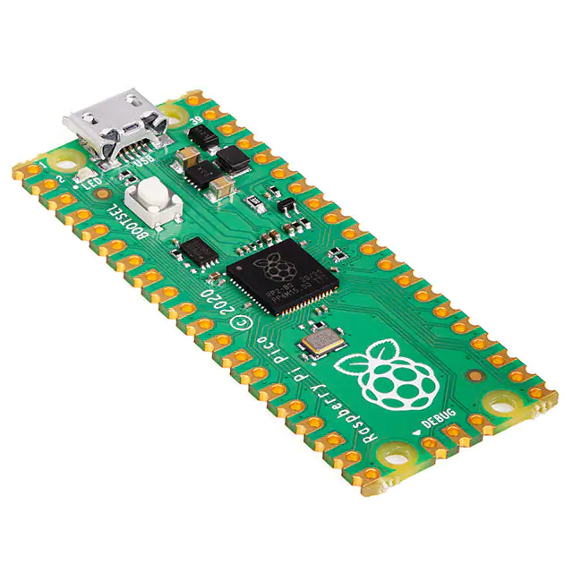
-
SC0915
Raspberry Pi
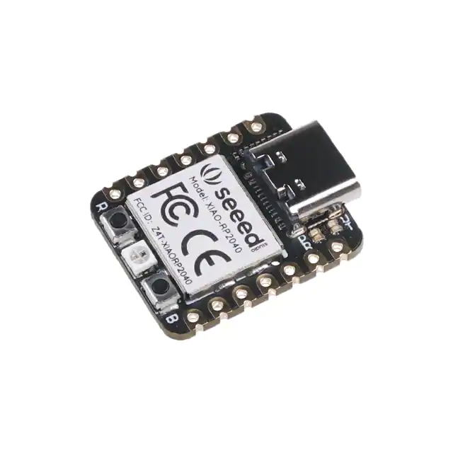
-
102010428
Seeed Technology Co., Ltd
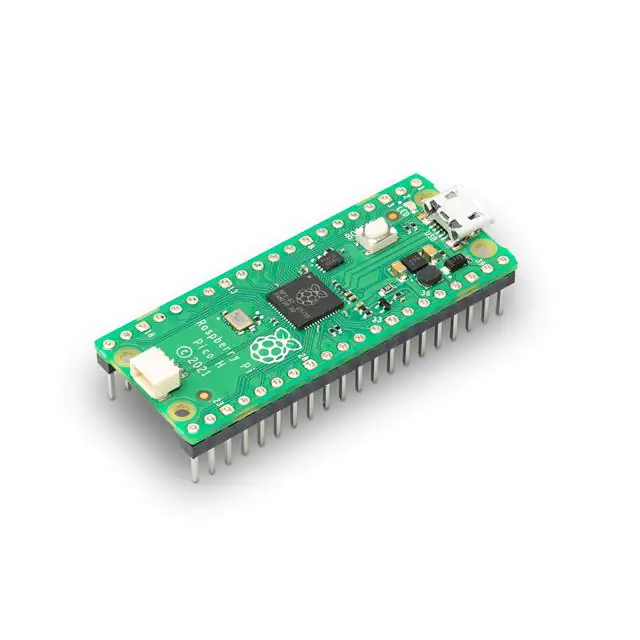
-
SC0917
Raspberry Pi

-
SC1631
Raspberry Pi
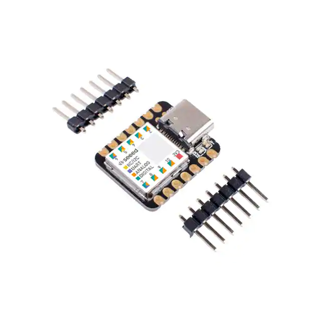
-
102010328
Seeed Technology Co., Ltd
-
102010388
Seeed Technology Co., Ltd
-
4600
Adafruit Industries LLC
-
102010268
Seeed Technology Co., Ltd
-
C124
M5Stack Technology Co., Ltd.
-
3500
Adafruit Industries LLC
-
5302
Adafruit Industries LLC
-
DFR0282
DFRobot
Tech Hub

A practical engineering and sourcing framework covering lifecycle verification, lifetime-buy calculations, replacement qualification, supplier checks and counterfeit-risk controls.

TTL and CMOS logic families differ in thresholds, loading, output drive, power and timing. This engineering guide compares 74HC and 74HCT, calculates noise margins and checks 3.3 V/5 V compatibility.

A practical engineering guide to 3.3V and 5V logic compatibility, input thresholds, resistor dividers, translator ICs, MOSFET level shifting, I2C pull-ups, timing limits and power-sequencing risks.

The 74HC595 uses push-pull logic outputs, while the TPIC6B595 uses 50 V open-drain DMOS sinks for higher-power loads. This guide compares timing, current limits, 3.3 V interfacing, load wiring, thermal…

The 74HC595 converts serial data into eight stable parallel outputs. This guide covers pin functions, shift and storage timing, OE and MR behavior, drive-current limits, cascading, voltage compatibilit…

A technical comparison of level-sensitive latches and edge-triggered flip-flops, covering timing windows, setup and hold limits, master–slave operation, time borrowing, race-through, HDL inference and…

A D latch stores one bit while Enable controls when data can pass. This reference covers gate-level operation, truth tables, transparency, setup and hold timing, LE versus OE, common ICs and practical …

An SR latch stores one bit through cross-coupled feedback. This engineering reference covers NOR and NAND implementations, truth tables, forbidden-state recovery, gated operation, switch debouncing, fa…

Latch circuits retain one bit through feedback. This technical reference covers SR and D latches, truth tables, transparency, timing limits, latch-versus-flip-flop behavior, applications and common log…

An engineering guide to LED driver operation, constant-current and constant-voltage outputs, linear and switching topologies, dimming, IC selection, calculations, replacement compatibility, and fault c…


