
 My Inquiry
 My Account


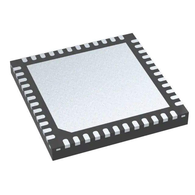
STMicroelectronics STM32WB55REV7
- Part No.:
- STM32WB55REV7
- Manufacturer:
- STMicroelectronics
- Category:
- RF Transceiver ICs
- Package:
- 68-VFQFN Exposed Pad
- Datasheet:
-
 STM32WB55REV7.pdf
- Description:
- IC RF TXRX+MCU 802.15.4 68VFQFPN
- Quantity:
- Payment:

- Shipping:

Inventory:2,120
Please send an inquiry. Send us your inquiry, and we will respond immediately.
Product details
Overview
STM32WB55REV7 from STMicroelectronics is a dual-core multiprotocol wireless 32-bit MCU integrating an Arm® Cortex®-M4 with FPU (64 MHz) and a dedicated Cortex®-M0+ radio controller, supporting Bluetooth® 5.4 and IEEE 802.15.4 PHY/MAC (Thread 1.3, Zigbee® 3.0). It delivers -96 dBm RX sensitivity (BLE 1 Mbps), +6 dBm programmable TX power, and ultra-low-power operation down to 13 nA in shutdown mode. Used in battery-powered IoT edge nodes requiring secure over-the-air updates and regulatory-compliant RF performance.
For engineers reviewing the STM32WB55REV7 datasheet, STM32WB55REV7 pinout, STM32WB55REV7 application, or STM32WB55REV7 equivalent, key selection criteria include dual-CPU real-time radio coexistence, integrated SMPS efficiency (<53 µA/MHz active), hardware AES-256 and PKA acceleration, and UFBGA129 package compatibility with industrial temperature range (-40 °C to 105 °C).
Technical Context
The device implements a tightly coupled dual-CPU architecture: the M4 executes application firmware while the M0+ handles time-critical BLE/802.15.4 link-layer operations via IPCC interprocessor messaging. Radio subsystem includes integrated balun, RSSI-based TX power control, and support for external PA or IPD matching (e.g., MLPF-WB55-02E3).
Power management features an embedded SMPS with intelligent bypass mode, five selectable BOR thresholds, and seven low-power modes - including Stop mode with 256 KB RAM retention at 2.1 µA. Clock system combines 32 MHz crystal (radio/CPU), 32 kHz LSE (RTC), and auto-trimmed MSI (±0.25% accuracy).
Key Specifications
| Parameter | Value and Actual Design Meaning |
|---|---|
| CPU Cores | Dual-core: Arm Cortex-M4 @ 64 MHz (FPU, ART Accelerator) + Cortex-M0+ @ 32 MHz (dedicated radio stack) |
| Wireless Protocols | Bluetooth 5.4 (LE), IEEE 802.15.4-2011 PHY/MAC - enabling Thread 1.3 and Zigbee 3.0 certified stacks |
| RF Performance | RX sensitivity: -96 dBm (BLE 1 Mbps), -100 dBm (802.15.4); TX output: programmable up to +6 dBm in 1 dB steps |
| Memory | 1 MB flash (PCROP-protected sectors), 256 KB SRAM (64 KB with hardware parity) |
| Power Consumption | 13 nA shutdown, 600 nA standby + RTC + 32 KB RAM, 2.1 µA stop + RTC + 256 KB RAM |
| Security | 3× AES-256 engines, HW PKA (RSA/ECC/DH), TRNG, 96-bit unique ID, Secure Firmware Installation (SFI) |
| Package | UFBGA129, 0.5 mm pitch, 7 × 7 mm body - suitable for high-density PCB layouts with thermal pad grounding |
Pinout & Package
STM32WB55REV7 is housed in a 129-ball UFBGA package (0.5 mm pitch, 7 × 7 mm footprint) with exposed thermal pad. Pin functions are validated per ST's DS11929 Rev 18, Section 4 ("Pinouts and pin description") and Table 16 ("STM32WB55xx pin and ball definitions").
| Pin/Terminal | Circuit Role | Design Meaning |
|---|---|---|
| VDD, VDDA, VDDRF | Power supply inputs | Separate domains for digital core (VDD), analog (VDDA), and RF (VDDRF) enable noise isolation and optimized regulation |
| VBAT | Backup power input | Supplies RTC and 32 backup registers during main power loss - supports coin-cell or supercap integration |
| PA0–PA15, PB0–PB15, PC0–PC15, PD0–PD2, PE0–PE7, PF0–PF1 | General-purpose I/Os | 72 fast I/Os total; 70 are 5 V-tolerant - simplifies level-shifting in mixed-voltage systems |
| RF_P, RF_N | Differential RF transceiver interface | Direct connection to antenna or external PA/IPD; requires impedance-matched 50 Ω layout per RF design guidelines |
| OSC_IN/OSC_OUT | 32 MHz crystal oscillator terminals | Drives both CPU and radio clocks; internal trimming capacitors eliminate external load caps |
| LSE_IN/LSE_OUT | 32 kHz RTC crystal terminals | Enables precise calendar timekeeping and low-power wake-up timing independent of main clock |
Key Features
| Feature | Design Value |
|---|---|
| Dual-CPU Real-Time Radio Isolation | M0+ offloads BLE/802.15.4 link layer, freeing M4 for application logic without RTOS scheduling overhead |
| Integrated RF Front-End | Built-in balun reduces BOM count and layout complexity; supports 2 Mbps data rate and advertising extensions |
| Ultra-Low-Power SMPS | Embedded step-down converter achieves <53 µA/MHz active current - critical for multi-year battery life in sensors |
| Hardware Security Subsystem | AES-256, PKA, and SFI enable secure OTA updates and cryptographic key management without software-side vulnerabilities |
| Quad-SPI with XIP | External flash execution capability eliminates boot latency and expands code space beyond on-chip 1 MB flash |
Applications
| Smart Home Sensor Hub | Industrial Wireless Node |
|---|---|
Use Scenario: Battery-powered multi-sensor node aggregating temperature, humidity, and motion data across BLE and Thread networks. IC Role / Device Role / Timing Role: Dual-core MCU acts as protocol gateway and local decision engine; M0+ handles concurrent BLE advertising and Thread mesh routing. Use Value: Integrated RF eliminates discrete transceiver BOM; -96 dBm sensitivity ensures reliable 30+ meter indoor range at 0 dBm TX. | Use Scenario: Predictive maintenance sensor deployed in factory machinery with 10-year battery target and ETSI/FCC compliance. IC Role / Device Role / Timing Role: Primary controller executing vibration analysis algorithms while maintaining low-duty-cycle 802.15.4 beaconing. Use Value: 2.1 µA Stop mode + RTC preserves timestamped event logs; SMPS efficiency extends battery life beyond 120 months. |
| Medical Wearable | Asset Tracking Tag |
Use Scenario: FDA-classified wearable monitoring heart rate and SpO₂, transmitting encrypted data via BLE to smartphone or gateway. IC Role / Device Role / Timing Role: Security-critical host processor managing biometric ADC sampling, AES-256 encryption, and BLE GATT caching. Use Value: Hardware TRNG and PKA accelerate certificate-based authentication; 64 KB SRAM with parity prevents memory corruption in safety-critical contexts. | Use Scenario: GPS-denied logistics tag reporting location via BLE beacons and periodic 802.15.4 uploads to LoRaWAN gateways. IC Role / Device Role / Timing Role: Dual-protocol coordinator synchronizing low-power GPS fix acquisition with scheduled RF transmissions. Use Value: EATT (Enhanced ATT) enables efficient bulk transfer of location history; RSSI-based TX power control minimizes interference in dense deployments. |
Equivalent & Alternatives
The following parts are listed as comparable options for similar dual-core wireless MCU applications.
| Alternative Part | Technical Difference | Application Difference | Selection Advice |
|---|---|---|---|
| Nordic nRF52840 | Single-core ARM Cortex-M4F @ 64 MHz; no dedicated radio CPU - BLE/802.15.4 handled in software stack | Limited real-time determinism for concurrent protocols; higher CPU load under multi-protocol operation | Preferred when BLE-only use case dominates and cost sensitivity outweighs dual-CPU determinism needs |
| TI CC2652R | Arm Cortex-M4F @ 48 MHz + dedicated Sensor Controller; supports BLE 5.0 and IEEE 802.15.4 but not Thread 1.3 out-of-box | Requires additional SDK licensing for Thread; lower max TX power (+5 dBm vs. +6 dBm) | Selected where TI ecosystem tooling and long-term production stability are prioritized over latest protocol versions |
Compared with nRF52840 and CC2652R, STM32WB55REV7 uniquely delivers hardware-isolated dual-CPU execution for deterministic BLE + Thread coexistence, +6 dBm TX headroom for marginal link budgets, and integrated SMPS for sub-µA standby - making it optimal for complex, battery-constrained, multi-protocol edge devices.
Availability
STM32WB55REV7 is available at Aetrix Electronics and suitable for smart home sensor hubs, industrial wireless nodes, medical wearables, and asset tracking tags requiring stable component supply, full production status (DS11929 Rev 18), and ECOPACK2-compliant packaging.
Supply support for STM32WB55REV7 includes scheduled delivery planning, volume procurement assistance, BOM continuity management, traceable sourcing, and lifecycle availability coordination for OEM customers, industrial embedded developers, connected-device designers, and electronics production programs.
Manufacturer
STMicroelectronics is a global semiconductor leader headquartered in Geneva, Switzerland, designing and manufacturing microcontrollers, power ICs, sensors, and automotive-grade components since 1987.
The STM32WB series targets secure, low-power wireless IoT endpoints - combining dual-core processing, multi-protocol RF, and hardware security to simplify certification and reduce time-to-market for FCC/ETSI-compliant devices.
FAQ
What is the maximum operating temperature range for STM32WB55REV7?
The STM32WB55REV7 is rated for industrial operation from -40 °C to 105 °C ambient temperature, validated per DS11929 Rev 18 Section 6.3.2. This extended range supports deployment in harsh environments such as factory floors, outdoor infrastructure, and automotive under-hood applications where thermal stability is critical.
Does STM32WB55REV7 support over-the-air (OTA) firmware updates?
Yes - STM32WB55REV7 supports secure OTA updates for both Bluetooth Low Energy and 802.15.4 stacks via its built-in bootloader. Updates leverage hardware AES-256 encryption and Secure Firmware Installation (SFI) to authenticate and decrypt payloads before flash programming, preventing unauthorized firmware injection.
Which external passive components are required for RF matching?
ST recommends companion IPD chips MLPF-WB55-02E3 or MLPF-WB-02D3 for optimized 2.4 GHz matching. These integrate balun, harmonics filter, and impedance transformer - eliminating discrete inductors/capacitors. If using discrete matching, DS11929 Rev 18 Table 5 specifies 0201-size 1.2 nH inductor and 0.8 pF capacitor for reference designs.
Can STM32WB55REV7 operate without an external 32 MHz crystal?
No - the 32 MHz crystal is mandatory for RF operation and CPU clocking. The internal 16 MHz RC oscillator lacks the ±20 ppm stability required by Bluetooth 5.4 and 802.15.4 standards. DS11929 Rev 18 Section 3.10 confirms the 32 MHz HSE is used for both radio timing and system clock generation.
STM32WB55REV7 Specifications
- Product attributes
- Attribute value
- Manufacturer:
- STMicroelectronics
- Series:
- STM32WB
- Package/Case:
- 68-VFQFN Exposed Pad
- Packaging:
- Tray
- Product Status:
- Active
- Programmable:
- Not Verified
- Type:
- TxRx + MCU
- RF Family/Standard:
- 802.15.4, Bluetooth
- Protocol:
- Bluetooth v5.3, Thread, Zigbee®
- Modulation:
- GFSK
- Frequency:
- 2.405GHz ~ 2.48GHz
- Data Rate (Max):
- 2Mbps
- Power - Output:
- 6dBm
- Sensitivity:
- -100dBm
- Memory Size:
- 512kB Flash, 256kB SRAM
- Serial Interfaces:
- ADC, I2C, SPI, UART, USART, USB
- GPIO:
- 49
- Voltage - Supply:
- 1.71V ~ 3.6V
- Current - Receiving:
- 4.5mA ~ 7.9mA
- Current - Transmitting:
- 5.2mA ~ 12.7mA
- Operating Temperature:
- -40°C ~ 105°C (TA)
- Grade:
- -
- Qualification:
- -
- Supplier Device Package:
- 68-VFQFPN (8x8)
STM32WB55REV7 FAQ
1.How can I place an order for STM32WB55REV7 through Aetrix?
Please submit a Request for Quotation (RFQ) for STM32WB55REV7 on Aetrix. Our sales agent will provide a competitive quotation and guide you through the order confirmation once you accept the terms.
2.Are the price and stock information for STM32WB55REV7 reliable?
The price and inventory of STM32WB55REV7 are updated periodically and may fluctuate due to market conditions. Stock and pricing data are typically refreshed every 24 hours. Quotation validity for STM32WB55REV7 is usually 5 days.
3.What payment methods are accepted for STM32WB55REV7?
We accept Wire Transfer, PayPal, Credit Card, Western Union, MoneyGram, and Escrow for STM32WB55REV7 transactions.
Note: Certain payment methods may incur a processing fee.
4.How is shipping managed for STM32WB55REV7?
STM32WB55REV7 orders can be shipped via leading logistics carriers, including DHL, UPS, FedEx, TNT, or Registered Mail.
Once your STM32WB55REV7 order is processed, you will receive an email with the shipment details and tracking number.
Note: Tracking information may take up to 24 hours to appear. Express delivery typically takes 3–5 business days.
5.How can I obtain technical support or documentation for STM32WB55REV7?
For technical support, including STM32WB55REV7 datasheets, pinout diagrams, or application guidance, please contact our engineering support team. They can provide detailed documentation and assistance for your STM32WB55REV7 requirements.
6.How does Aetrix verify that STM32WB55REV7 is sourced from the original manufacturer or authorized distributors?
All STM32WB55REV7 products on Aetrix are procured from qualified distributors and authorized channels. Our dedicated quality assurance team conducts strict verification, including traceability checks and, if necessary, third-party testing. This ensures that STM32WB55REV7 meets industry standards.
7.What is the process for return or replacement of STM32WB55REV7?
All STM32WB55REV7 units undergo pre-shipment inspection (PSI). If there is an issue with STM32WB55REV7, returns or replacements are accepted under the following conditions:
1.Quantity discrepancies, incorrect items, or visible external defects (such as breakage or corrosion), acknowledged by Aetrix.
2.The issue is reported within 90 days of delivery.
3.The STM32WB55REV7 part is unused and in its original packaging.
Return procedure for STM32WB55REV7:
1.Submit a request within 90 days.
2.Obtain a Return Material Authorization (RMA) from Aetrix.
STM32WB55REV7 Tags

-
ESP32-D0WD-V3
Espressif Systems

-
ESP8266EX
Espressif Systems

-
ESP32-S3
Espressif Systems

-
NRF24L01P-R7
Nordic Semiconductor ASA
-
NRF24L01P-R
Nordic Semiconductor ASA

-
ESP32-U4WDH
Espressif Systems

-
DA14531-00000OG2
Renesas
-
ESP32-C6FH4
Espressif Systems

-
DA14531-00000FX2
Renesas
-
NRF24L01P-T
Nordic Semiconductor ASA

-
NRF52810-QCAA-R
Nordic Semiconductor ASA
-
ESP32-S3FN8
Espressif Systems
Tech Hub

A practical engineering and sourcing framework covering lifecycle verification, lifetime-buy calculations, replacement qualification, supplier checks and counterfeit-risk controls.

TTL and CMOS logic families differ in thresholds, loading, output drive, power and timing. This engineering guide compares 74HC and 74HCT, calculates noise margins and checks 3.3 V/5 V compatibility.

A practical engineering guide to 3.3V and 5V logic compatibility, input thresholds, resistor dividers, translator ICs, MOSFET level shifting, I2C pull-ups, timing limits and power-sequencing risks.

The 74HC595 uses push-pull logic outputs, while the TPIC6B595 uses 50 V open-drain DMOS sinks for higher-power loads. This guide compares timing, current limits, 3.3 V interfacing, load wiring, thermal…

The 74HC595 converts serial data into eight stable parallel outputs. This guide covers pin functions, shift and storage timing, OE and MR behavior, drive-current limits, cascading, voltage compatibilit…

A technical comparison of level-sensitive latches and edge-triggered flip-flops, covering timing windows, setup and hold limits, master–slave operation, time borrowing, race-through, HDL inference and…

A D latch stores one bit while Enable controls when data can pass. This reference covers gate-level operation, truth tables, transparency, setup and hold timing, LE versus OE, common ICs and practical …

An SR latch stores one bit through cross-coupled feedback. This engineering reference covers NOR and NAND implementations, truth tables, forbidden-state recovery, gated operation, switch debouncing, fa…

Latch circuits retain one bit through feedback. This technical reference covers SR and D latches, truth tables, transparency, timing limits, latch-versus-flip-flop behavior, applications and common log…

An engineering guide to LED driver operation, constant-current and constant-voltage outputs, linear and switching topologies, dimming, IC selection, calculations, replacement compatibility, and fault c…


