
 My Inquiry
 My Account


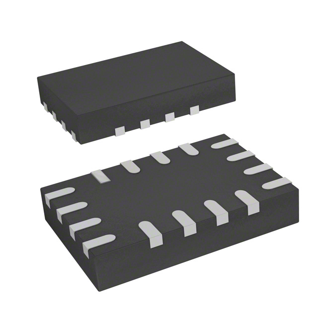
STMicroelectronics STMPE801QTR
- Part No.:
- STMPE801QTR
- Manufacturer:
- STMicroelectronics
- Category:
- I/O Expanders
- Package:
- 16-UFQFN
- Datasheet:
-
 STMPE801QTR.pdf
- Description:
- IC XPNDR 400KHZ I2C 16QFN
- Quantity:
- Payment:

- Shipping:

Inventory:3,980
Please send an inquiry. Send us your inquiry, and we will respond immediately.
Product details
Overview
STMPE801QTR from STMicroelectronics is an 8-bit I²C GPIO port expander IC designed to extend digital ASIC I/O resources in space-constrained mobile multimedia platforms. It features 8 configurable GPIOs, dual supply rails (VCC 1.65–3.6 V, VIO 1.65–3.6 V), <1 µA suspend current, interrupt output, and hardware reset input - enabling low-power touch/keypad interface in portable media players and smartphones.
For engineers reviewing the STMPE801QTR datasheet, STMPE801QTR pinout, STMPE801QTR application, or STMPE801QTR equivalent, key selection considerations include I²C address configurability (0x82/0x88), per-pin wake-up capability, independent VIO/VCC level-shifting, and QFN16L (2.6 mm × 1.8 mm) package suitability for high-density PCB layouts.
Technical Context
The STMPE801QTR implements a dedicated I²C slave interface compliant with Philips I²C Specification v2.1, supporting standard (100 kbps) and fast-mode (400 kbps) operation. Its register-mapped architecture includes system control (soft reset, I²C shutdown), GPIO direction/state/monitor registers, and interrupt enable/status registers - all accessible via sequential or random I²C reads/writes with auto-increment support.
Each of the eight GPIOs can be individually configured as input or output, with interrupt generation on logic transition. The device supports two-device bus sharing via a single address line (ADDR0), and incorporates hardware-level power optimization: I²C block shutdown (via I2C_SHDN bit) reduces current to minimum, while VIO-powered GPIOs remain functional even when VCC is off - provided VIO ≥ VCC.
Key Specifications
| Parameter | Value and Actual Design Meaning |
|---|---|
| GPIO count | 8 bidirectional, individually configurable pins for keypad, LED, or sensor interface expansion |
| I²C address options | 0x82 or 0x88 (ADDR0 pin-selectable), enabling dual-device bus sharing without address conflict |
| Suspend current | <1 µA - enables ultra-low-power standby in battery-operated portable devices |
| VIO / VCC range | 1.65 V – 3.6 V each, with VIO ≥ VCC - supports level-shifting between host processor and peripheral voltage domains |
| Interrupt output | Active-low open-drain INT pin - signals GPIO state change to host CPU without polling overhead |
| Reset input | Asynchronous active-low RESET pin (min. 100 µs pulse) - provides deterministic hardware initialization |
| ESD protection | 2 kV HBM on each GPIO - enhances robustness against electrostatic discharge in handheld environments |
Pinout & Package
STMPE801QTR is housed in a 16-pin QFN package (2.6 mm × 1.8 mm, 0.4 mm pitch) with exposed thermal pad, optimized for compact mobile PCBs and efficient heat dissipation.
| Pin/Terminal | Circuit Role | Design Meaning |
|---|---|---|
| 1 (INT) | Interrupt output | Open-drain signal indicating GPIO state change; requires external pull-up for host CPU edge detection |
| 2 (RESET) | Reset input | Asynchronous active-low reset; asserts internal POR and forces all GPIOs to input state |
| 3 (CLOCK) | I²C clock (SCL) | Input-only clock line; supports up to 400 kHz fast-mode timing with defined tLOW/tHIGH constraints |
| 4 (ADDRESS) | I²C address select | Configures slave address to 0x82 (low) or 0x88 (high); enables dual-device bus topology |
| 5 (DATA) | I²C data (SDA) | Open-drain bidirectional data line; complies with I²C bus electrical requirements (VOL/VOH, tSU/tHD) |
| 6 (VCC) | I²C logic supply | Powers I²C interface block only; may be powered down independently of VIO to reduce leakage |
| 7 (VIO) | GPIO I/O supply | Defines logic thresholds and drive strength for all 8 GPIOs; must be ≥ VCC for proper level shifting |
| 8 (GND) | Ground reference | Common return path for VCC, VIO, and GPIO signals; connects to thermal pad for thermal management |
| 9–16 (GPIO_0–GPIO_7) | General-purpose I/O | Configurable as input (with interrupt/wake-up), output (push-pull), or high-impedance; default to input on reset |
Key Features
| Feature | Design Value |
|---|---|
| Per-GPIO wake-up | Each GPIO generates interrupt on rising/falling edge - eliminates continuous polling and extends battery life |
| Independent VIO/VCC rails | VIO powers GPIOs, VCC powers I²C logic - allows host to shut down I²C block while retaining GPIO monitoring |
| I²C block shutdown | Writing '1' to I2C_SHDN bit disables I²C interface on next clock edge - reduces current to sub-µA suspend state |
| Register auto-increment | Sequential read/write across GPIO monitor/set/direction registers (0x10–0x12) - minimizes I²C transaction overhead |
| Hardware reset recovery | RESET pin assertion clears all registers and reinitializes GPIOs to input mode - ensures deterministic startup after brownout |
Applications
| Keypad Interface | Touch Panel Control |
|---|---|
|
Use Scenario: Matrix keypad scanning in smartphone front panel with limited ASIC GPIOs. IC Role / Device Role / Timing Role: GPIO expander providing 8 programmable lines for row/column scanning and interrupt-driven key press detection. Use Value: Reduces host CPU polling load by generating INT on key press/release, enabling immediate response and lower average power consumption. |
Use Scenario: Resistive touch panel coordinate acquisition in portable media player. IC Role / Device Role / Timing Role: Configurable GPIOs used to drive touch panel X/Y electrodes and read analog sense lines via external ADC interface. Use Value: Enables precise timing control of electrode switching sequences and synchronized interrupt signaling upon touch detection. |
| LED Status Indication | System Power Management |
|
Use Scenario: Multi-color status LED control in game console UI with dynamic brightness adjustment. IC Role / Device Role / Timing Role: GPIO outputs driving LED anodes/cathodes; software-configurable as push-pull outputs with 8 mA sink/source capability. Use Value: Eliminates need for discrete transistors or LED drivers; supports rapid on/off toggling via register writes without I²C protocol overhead. |
Use Scenario: Monitoring battery charge status and peripheral readiness in smart phone baseband subsystem. IC Role / Device Role / Timing Role: GPIO inputs monitoring charger detect, USB VBUS presence, and accessory insertion signals - all with wake-up capability. Use Value: Allows baseband SoC to remain in deep sleep until critical event occurs, reducing system-wide quiescent current by >50%. |
Equivalent & Alternatives
The following parts are listed as comparable options for similar GPIO expansion applications.
| Alternative Part | Technical Difference | Application Difference | Selection Advice |
|---|---|---|---|
| TCA6408A | 8-bit I²C expander with identical VIO/VCC range (1.65–3.6 V), but no per-pin wake-up; fixed I²C address (0x20–0x27) | Lacks individual GPIO interrupt masking and wake-up - requires host polling or global interrupt handling | Select when cost sensitivity outweighs per-pin event detection needs and bus address flexibility is not required. |
| PCA9538 | 8-bit I²C expander with 2.3–5.5 V VCC range, integrated pull-ups, but no VIO rail separation - no level-shifting capability | Cannot interface mixed-voltage systems (e.g., 1.8 V host + 3.3 V peripherals) without external level shifters | Choose for legacy 3.3 V–5 V systems where voltage domain isolation is unnecessary and board space permits external components. |
Compared with TCA6408A and PCA9538, STMPE801QTR uniquely delivers per-GPIO wake-up, dual-supply level shifting, and I²C block shutdown - making it optimal for battery-critical, multi-voltage mobile designs requiring minimal host intervention and maximal power autonomy.
Availability
STMPE801QTR is available at Aetrix Electronics and suitable for portable media players, smartphones, and game consoles requiring stable component supply, long-term lifecycle support, and RoHS-compliant QFN packaging.
Supply support for STMPE801QTR includes scheduled delivery planning, volume procurement assistance, BOM continuity management, traceable sourcing, and lifecycle availability coordination for OEM customers, industrial embedded developers, connected-device designers, and electronics production programs.
Manufacturer
STMicroelectronics is a global semiconductor leader headquartered in Geneva, Switzerland, specializing in microcontrollers, power management, sensors, and analog ICs for automotive, industrial, and consumer markets.
The STMPE series targets mobile multimedia platforms, delivering highly integrated, low-power peripheral interface solutions - specifically engineered to resolve I/O scarcity in space- and power-constrained handheld devices.
FAQ
What is the function of the VIO pin, and why must it be ≥ VCC?
VIO supplies power to the GPIO I/O buffers and defines their logic thresholds and drive strength. It must be ≥ VCC because the internal level-shifting circuitry relies on VIO as the higher reference to ensure correct signal translation between the I²C logic block (powered by VCC) and the GPIO pins. Violating this condition risks undefined output states or latch-up.
Can the STMPE801QTR operate with only VIO powered and VCC disconnected?
Yes - the GPIOs remain fully functional with only VIO powered, as the I²C interface (VCC-powered) is isolated. However, I²C communication is disabled. This mode supports always-on GPIO monitoring (e.g., wake-up detection) while the host processor's I²C master is powered down, achieving ultra-low system standby current.
How does the I²C block shutdown feature work, and how is it re-enabled?
Writing '1' to the I2C_SHDN bit in the SystemControl register disables the I²C interface on the next SCL clock edge, dropping current to <1 µA. Re-enabling requires a hardware RESET pulse (≥100 µs) to reinitialize the I²C state machine - software-only recovery is not supported, ensuring deterministic restart behavior.
Is the INT pin active-high or active-low, and what drives its output state?
The INT pin is active-low, open-drain, and asserted when any enabled GPIO transitions (rising/falling edge). It remains low until the host reads the ISGPIOR register - which clears the corresponding status bit and releases INT. External pull-up is mandatory; typical value is 4.7 kΩ to VIO.
STMPE801QTR Specifications
- Product attributes
- Attribute value
- Manufacturer:
- STMicroelectronics
- Series:
- Xpander Logic™
- Package/Case:
- 16-UFQFN
- Packaging:
- Tape & Reel (TR)
- Product Status:
- Obsolete
- Programmable:
- Not Verified
- Number of I/O:
- 8
- Interface:
- I2C
- Interrupt Output:
- Yes
- Features:
- POR
- Output Type:
- Push-Pull
- Current - Output Source/Sink:
- -
- Clock Frequency:
- 400 kHz
- Voltage - Supply:
- 1.65V ~ 3.6V
- Operating Temperature:
- -40°C ~ 85°C
- Grade:
- -
- Qualification:
- -
- Mounting Type:
- Surface Mount
- Supplier Device Package:
- 16-QFN (2.6x1.8)
STMPE801QTR FAQ
1.How can I place an order for STMPE801QTR through Aetrix?
Please submit a Request for Quotation (RFQ) for STMPE801QTR on Aetrix. Our sales agent will provide a competitive quotation and guide you through the order confirmation once you accept the terms.
2.Are the price and stock information for STMPE801QTR reliable?
The price and inventory of STMPE801QTR are updated periodically and may fluctuate due to market conditions. Stock and pricing data are typically refreshed every 24 hours. Quotation validity for STMPE801QTR is usually 5 days.
3.What payment methods are accepted for STMPE801QTR?
We accept Wire Transfer, PayPal, Credit Card, Western Union, MoneyGram, and Escrow for STMPE801QTR transactions.
Note: Certain payment methods may incur a processing fee.
4.How is shipping managed for STMPE801QTR?
STMPE801QTR orders can be shipped via leading logistics carriers, including DHL, UPS, FedEx, TNT, or Registered Mail.
Once your STMPE801QTR order is processed, you will receive an email with the shipment details and tracking number.
Note: Tracking information may take up to 24 hours to appear. Express delivery typically takes 3–5 business days.
5.How can I obtain technical support or documentation for STMPE801QTR?
For technical support, including STMPE801QTR datasheets, pinout diagrams, or application guidance, please contact our engineering support team. They can provide detailed documentation and assistance for your STMPE801QTR requirements.
6.How does Aetrix verify that STMPE801QTR is sourced from the original manufacturer or authorized distributors?
All STMPE801QTR products on Aetrix are procured from qualified distributors and authorized channels. Our dedicated quality assurance team conducts strict verification, including traceability checks and, if necessary, third-party testing. This ensures that STMPE801QTR meets industry standards.
7.What is the process for return or replacement of STMPE801QTR?
All STMPE801QTR units undergo pre-shipment inspection (PSI). If there is an issue with STMPE801QTR, returns or replacements are accepted under the following conditions:
1.Quantity discrepancies, incorrect items, or visible external defects (such as breakage or corrosion), acknowledged by Aetrix.
2.The issue is reported within 90 days of delivery.
3.The STMPE801QTR part is unused and in its original packaging.
Return procedure for STMPE801QTR:
1.Submit a request within 90 days.
2.Obtain a Return Material Authorization (RMA) from Aetrix.
STMPE801QTR Tags
-
TCA6408ARSVR
Texas Instruments

-
TCA9535RTWR
Texas Instruments
-
FXL6408UMX
onsemi

-
PCF8574ADWR
Texas Instruments

-
PCF8574APWR
Texas Instruments
-
TCA9555PWR
Texas Instruments

-
TCA9554PWR
Texas Instruments
-
TCA9554APWR
Texas Instruments

-
TCA9539PWR
Texas Instruments
-
TCA9534PWR
Texas Instruments
-
TCA9555RTWR
Texas Instruments
-
TCA9535PWR
Texas Instruments
Tech Hub

A practical engineering and sourcing framework covering lifecycle verification, lifetime-buy calculations, replacement qualification, supplier checks and counterfeit-risk controls.

TTL and CMOS logic families differ in thresholds, loading, output drive, power and timing. This engineering guide compares 74HC and 74HCT, calculates noise margins and checks 3.3 V/5 V compatibility.

A practical engineering guide to 3.3V and 5V logic compatibility, input thresholds, resistor dividers, translator ICs, MOSFET level shifting, I2C pull-ups, timing limits and power-sequencing risks.

The 74HC595 uses push-pull logic outputs, while the TPIC6B595 uses 50 V open-drain DMOS sinks for higher-power loads. This guide compares timing, current limits, 3.3 V interfacing, load wiring, thermal…

The 74HC595 converts serial data into eight stable parallel outputs. This guide covers pin functions, shift and storage timing, OE and MR behavior, drive-current limits, cascading, voltage compatibilit…

A technical comparison of level-sensitive latches and edge-triggered flip-flops, covering timing windows, setup and hold limits, master–slave operation, time borrowing, race-through, HDL inference and…

A D latch stores one bit while Enable controls when data can pass. This reference covers gate-level operation, truth tables, transparency, setup and hold timing, LE versus OE, common ICs and practical …

An SR latch stores one bit through cross-coupled feedback. This engineering reference covers NOR and NAND implementations, truth tables, forbidden-state recovery, gated operation, switch debouncing, fa…

Latch circuits retain one bit through feedback. This technical reference covers SR and D latches, truth tables, transparency, timing limits, latch-versus-flip-flop behavior, applications and common log…

An engineering guide to LED driver operation, constant-current and constant-voltage outputs, linear and switching topologies, dimming, IC selection, calculations, replacement compatibility, and fault c…


