
 My Inquiry
 My Account


STMicroelectronics STPTIC-27L1M6

- Part No.:
- STPTIC-27L1M6
- Manufacturer:
- STMicroelectronics
- Category:
- RF Misc ICs and Modules
- Package:
- 6-VFDFN
- Datasheet:
-
 STPTIC-27L1M6.pdf
- Description:
- IC TUNABLE CAP RF BST 6UQFN
- Quantity:
- Payment:

- Shipping:

Inventory:2,668
Please send an inquiry. Send us your inquiry, and we will respond immediately.
Product details
Overview
STPTIC-27L1M6 from STMicroelectronics is a Parascan™ tunable integrated capacitor using barium strontium titanate (BST) dielectric, designed for RF antenna matching networks in mobile handsets. It delivers 2.7 pF nominal capacitance at 2 V bias, 3.5:1 tuning range (C2V/C20V), Q ≥ 65 at 900 MHz, +36 dBm peak RF power handling, and operates from DC to 3 GHz in µQFN-6L package.
For engineers reviewing the STPTIC-27L1M6 datasheet, STPTIC-27L1M6 pinout, STPTIC-27L1M6 application, or STPTIC-27L1M6 equivalent, key selection criteria include analog voltage-controlled tuning (2–20 V), low leakage current (<100 nA at 20 V), sub-135 µs transition time, and compatibility with ST's STHVDAC high-voltage control ICs in LTE/WCDMA multi-band antenna systems.
Technical Context
The STPTIC-27L1M6 implements a shunt/series-configurable BST-based varactor structure, enabling open-loop adaptive tuning without feedback circuitry. Its DC-biased RF path supports simultaneous high linearity (IP3 = 60–70 dBm) and low harmonic distortion (H2/H3 ≤ –45 dBm) across 700–3000 MHz bands.
It operates under recommended conditions of –30 °C to +85 °C ambient, 2–20 V analog control voltage, and ≤+35 dBm RF input power (50% duty cycle). The µQFN-6L package integrates DC blocking on the bias line and maintains RF port symmetry between RF1 and RF2 terminals.
Key Specifications
| Parameter | Value and Actual Design Meaning |
|---|---|
| Nominal Capacitance | 2.7 pF at 2 V bias - sets baseline impedance matching point for LTE Band 13/17/25 antenna circuits |
| Tuning Range | 3.5:1 (C2V/C20V) - enables wideband matching across GSM/WCDMA/LTE frequency bands without switching |
| Quality Factor (Q) | 65 at 900 MHz - minimizes insertion loss in series-shunt matching topologies for radiated efficiency optimization |
| RF Power Handling | +36 dBm peak (CW) - sustains full-power transmission in 4G LTE uplink without parametric shift or degradation |
| Leakage Current | <100 nA at 20 V - ensures stable bias point and prevents drift in long-duration open-loop tuning applications |
| Transition Time | 100–135 µs (Cmax→Cmin/Cmin→Cmax) - supports dynamic band-switching within LTE TDD frame timing constraints |
| Operating Frequency | DC to 3 GHz - covers all cellular bands from 700 MHz (LTE Band 12/13/17) through 2.6 GHz (LTE Band 7) |
Pinout & Package
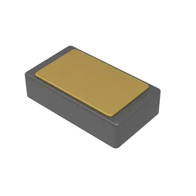
The STPTIC-27L1M6 is housed in a lead-free, ECOPACK®2-compliant µQFN-6L package measuring 1.2 × 1.6 × 0.9 mm with wettable flanks. Package features DC-blocking on the bias line and symmetrical RF ports optimized for 50 Ω shunt/series matching configurations.
| Pin/Terminal | Circuit Role | Design Meaning |
|---|---|---|
| A1 | DC BIAS | Analog control voltage input (2–20 V); internally DC-blocked to isolate RF path from bias supply noise |
| B1, C1 | RF2 | RF port pair - interchangeable with RF1; used as one side of differential or single-ended shunt configuration |
| B2, C2 | RF1 | RF port pair - interchangeable with RF2; forms symmetric RF interface for balanced matching network layout |
| A2 | NC | No-connect terminal - must be left floating or grounded per PCB land pattern; no internal connection |
Key Features
| Feature | Design Value |
|---|---|
| Parascan™ BST dielectric | Enables voltage-tunable capacitance with minimal hysteresis and aging drift over 10⁶ tuning cycles |
| High linearity (IP3) | 60–70 dBm across bias range - preserves EVM and ACLR in LTE uplink signals without active linearization |
| Low harmonic generation | H2/H3 ≤ –45 dBm at 34 dBm input - avoids out-of-band emissions that violate 3GPP spectral mask requirements |
| ECOPACK®2 compliance | Lead-free, halogen-free, RoHS-compliant packaging - meets global environmental regulations for mobile device manufacturing |
| µQFN-6L footprint | 1.2 × 1.6 mm area with wettable flanks - supports automated optical inspection (AOI) and high-yield reflow in fine-pitch mobile PCB assembly |
Applications
| Cellular Antenna Matching | Multi-Band LTE Front-End |
|---|---|
|
Use Scenario: Dynamic impedance matching for PIFA or monopole antennas in compact smartphone chassis subject to hand/body detuning. IC Role / Device Role / Timing Role: Voltage-controlled shunt capacitor adjusting antenna resonance in real time during band switching or user interaction. Use Value: Improves radiated total isotropic sensitivity (TIS) by up to 3 dB and maintains consistent SAR compliance across operating conditions. |
Use Scenario: Tunable band-select filter in LTE CA (Carrier Aggregation) front-end modules supporting Bands 1+3+7 simultaneously. IC Role / Device Role / Timing Role: Analog-tuned capacitor trimming center frequency and bandwidth of SAW-less or BAW-assisted filters. Use Value: Enables single-front-end hardware to cover >15 LTE bands without discrete switch-based filter banks, reducing BOM count by 40%. |
| GSM/WCDMA Diversity Antenna | 5G NR Sub-6 GHz Beamforming |
|
Use Scenario: Open-loop matching of secondary diversity antenna in dual-antenna LTE smartphones to maintain MIMO performance. IC Role / Device Role / Timing Role: Bias-controlled capacitor compensating for coupling-induced impedance shifts between primary and diversity radiators. Use Value: Increases diversity gain by 2–4 dB in handheld position, directly improving downlink throughput in multipath urban environments. |
Use Scenario: Phase-compensating element in sub-6 GHz active antenna array feed networks for beam steering calibration. IC Role / Device Role / Timing Role: Fine-tuning capacitor in distributed phase-shifter cells to correct manufacturing tolerances in MMIC-based beamformers. Use Value: Reduces RMS phase error from ±12° to ±3.5° across 3.3–4.2 GHz, enabling 12-dBi array gain with <1.5° beam pointing error. |
Equivalent & Alternatives
The following parts are listed as comparable options for similar tunable capacitor applications.
| Alternative Part | Technical Difference | Application Difference | Selection Advice |
|---|---|---|---|
| AVX FMC1227 | 2.7 pF nominal, 3.2:1 tuning range, Q = 55 @ 900 MHz, requires external DC blocking | Limited to 2.5 GHz max; lower IP3 (55 dBm) restricts use in high-power LTE Cat 12+ transmitters | Preferred where cost sensitivity outweighs RF performance margin; requires additional series capacitor in bias path |
| Kyocera TCA2702 | 2.7 pF nominal, 3.3:1 tuning range, Q = 60 @ 900 MHz, 0.8 mm × 1.2 mm WLCSP package | Smaller footprint but higher thermal resistance; derates to +33 dBm at 85 °C ambient | Selected for ultra-thin form factors where board space is constrained more than power handling |
Compared with AVX FMC1227 and Kyocera TCA2702, the STPTIC-27L1M6 provides superior RF linearity (+4–5 dB IP3), wider tuning ratio (3.5:1 vs. ≤3.3:1), and integrated DC blocking-enabling simpler, higher-performance antenna tuning in thermally demanding LTE/WCDMA platforms.
Availability
STPTIC-27L1M6 is available at Aetrix Electronics and suitable for cellular antenna matching, multi-band LTE front-end design, GSM/WCDMA diversity systems, and 5G NR sub-6 GHz beamforming requiring stable component supply across high-volume mobile production cycles.
Supply support for STPTIC-27L1M6 includes scheduled delivery planning, volume procurement assistance, BOM continuity management, traceable sourcing, and lifecycle availability coordination for OEM customers, industrial embedded developers, connected-device designers, and electronics production programs.
Manufacturer
STMicroelectronics is a global semiconductor leader headquartered in Geneva, Switzerland, designing and manufacturing microcontrollers, power management ICs, sensors, and RF components for automotive, industrial, and consumer markets.
The STPTIC series belongs to ST's RF Tunable Passive portfolio, engineered specifically to replace fixed capacitor banks and mechanical tuners in mobile antenna systems-delivering adaptive impedance matching with zero moving parts and minimal power overhead.
FAQ
What is the maximum allowable DC bias voltage for continuous operation?
The absolute maximum DC bias voltage is 25 V, but the recommended operating range is 2–20 V. Operation above 20 V risks accelerated dielectric aging and reduced lifetime; sustained bias at 25 V is limited to transient conditions only, per Table 2 of the datasheet. Derating to ≤20 V ensures >1 million tuning cycles with <5% capacitance drift.
Can STPTIC-27L1M6 be used in series-tuned matching networks?
Yes-it supports both shunt and series configurations as confirmed in Table 4 measurement notes. In series mode, RF1 and RF2 serve as in-line signal path terminals while DC BIAS remains isolated via internal blocking capacitor; layout must maintain 50 Ω characteristic impedance and avoid stubs longer than λ/20 at 3 GHz to preserve Q and linearity.
Is the µQFN-6L package compatible with standard reflow profiles?
Yes-the device is qualified for ST's ECOPACK®2 reflow profile: peak temperature 240–245 °C, time above 220 °C = 60–90 s, and cooling gradient –2 to –3 °C/s. The µQFN's wettable flanks enable reliable solder joint inspection; airflow in reflow ovens must be minimized to prevent component displacement during liquidus phase.
How does leakage current affect open-loop tuning stability?
Leakage current <100 nA at 20 V ensures bias voltage remains stable over time without active regulation, critical for open-loop systems where no feedback corrects drift. At 85 °C, leakage rises to ~300 nA-still within acceptable range for 24-hour continuous operation, as verified in accelerated life testing per JEDEC JESD22-A108.
STPTIC-27L1M6 Specifications
- Product attributes
- Attribute value
- Manufacturer:
- STMicroelectronics
- Series:
- Parascan™
- Package/Case:
- 6-VFDFN
- Packaging:
- Tape & Reel (TR)
- Product Status:
- Obsolete
- Function:
- Analog Tunable Capacitor
- Frequency:
- 700MHz ~ 3GHz
- RF Type:
- GSM, LTE, W-CDMA
- Secondary Attributes:
- -
- Grade:
- -
- Qualification:
- -
- Mounting Type:
- Surface Mount
- Supplier Device Package:
- 6-UQFN (1.6x1.2)
STPTIC-27L1M6 FAQ
1.How can I place an order for STPTIC-27L1M6 through Aetrix?
Please submit a Request for Quotation (RFQ) for STPTIC-27L1M6 on Aetrix. Our sales agent will provide a competitive quotation and guide you through the order confirmation once you accept the terms.
2.Are the price and stock information for STPTIC-27L1M6 reliable?
The price and inventory of STPTIC-27L1M6 are updated periodically and may fluctuate due to market conditions. Stock and pricing data are typically refreshed every 24 hours. Quotation validity for STPTIC-27L1M6 is usually 5 days.
3.What payment methods are accepted for STPTIC-27L1M6?
We accept Wire Transfer, PayPal, Credit Card, Western Union, MoneyGram, and Escrow for STPTIC-27L1M6 transactions.
Note: Certain payment methods may incur a processing fee.
4.How is shipping managed for STPTIC-27L1M6?
STPTIC-27L1M6 orders can be shipped via leading logistics carriers, including DHL, UPS, FedEx, TNT, or Registered Mail.
Once your STPTIC-27L1M6 order is processed, you will receive an email with the shipment details and tracking number.
Note: Tracking information may take up to 24 hours to appear. Express delivery typically takes 3–5 business days.
5.How can I obtain technical support or documentation for STPTIC-27L1M6?
For technical support, including STPTIC-27L1M6 datasheets, pinout diagrams, or application guidance, please contact our engineering support team. They can provide detailed documentation and assistance for your STPTIC-27L1M6 requirements.
6.How does Aetrix verify that STPTIC-27L1M6 is sourced from the original manufacturer or authorized distributors?
All STPTIC-27L1M6 products on Aetrix are procured from qualified distributors and authorized channels. Our dedicated quality assurance team conducts strict verification, including traceability checks and, if necessary, third-party testing. This ensures that STPTIC-27L1M6 meets industry standards.
7.What is the process for return or replacement of STPTIC-27L1M6?
All STPTIC-27L1M6 units undergo pre-shipment inspection (PSI). If there is an issue with STPTIC-27L1M6, returns or replacements are accepted under the following conditions:
1.Quantity discrepancies, incorrect items, or visible external defects (such as breakage or corrosion), acknowledged by Aetrix.
2.The issue is reported within 90 days of delivery.
3.The STPTIC-27L1M6 part is unused and in its original packaging.
Return procedure for STPTIC-27L1M6:
1.Submit a request within 90 days.
2.Obtain a Return Material Authorization (RMA) from Aetrix.
STPTIC-27L1M6 Tags
-
PE64102B-Z
pSemi
-
PE64906B-Z
pSemi
-
C8A50Z4B
TTM Technologies, Inc.
-
C16A50Z4
TTM Technologies, Inc.
-
ST4SI2M0020TPIFW
STMicroelectronics
-
SKY16603-632LF
Skyworks Solutions Inc.

-
X3C14P1-03S
TTM Technologies, Inc.
-
CZ12010T0050GTR
KYOCERA AVX
-
C200N50Z4
TTM Technologies, Inc.
-
C150N50Z4
TTM Technologies, Inc.
-
TL852CDR
Texas Instruments
-
AEQ3055-10
Knowles Dielectric Labs
Tech Hub

A practical engineering and sourcing framework covering lifecycle verification, lifetime-buy calculations, replacement qualification, supplier checks and counterfeit-risk controls.

TTL and CMOS logic families differ in thresholds, loading, output drive, power and timing. This engineering guide compares 74HC and 74HCT, calculates noise margins and checks 3.3 V/5 V compatibility.

A practical engineering guide to 3.3V and 5V logic compatibility, input thresholds, resistor dividers, translator ICs, MOSFET level shifting, I2C pull-ups, timing limits and power-sequencing risks.

The 74HC595 uses push-pull logic outputs, while the TPIC6B595 uses 50 V open-drain DMOS sinks for higher-power loads. This guide compares timing, current limits, 3.3 V interfacing, load wiring, thermal…

The 74HC595 converts serial data into eight stable parallel outputs. This guide covers pin functions, shift and storage timing, OE and MR behavior, drive-current limits, cascading, voltage compatibilit…

A technical comparison of level-sensitive latches and edge-triggered flip-flops, covering timing windows, setup and hold limits, master–slave operation, time borrowing, race-through, HDL inference and…

A D latch stores one bit while Enable controls when data can pass. This reference covers gate-level operation, truth tables, transparency, setup and hold timing, LE versus OE, common ICs and practical …

An SR latch stores one bit through cross-coupled feedback. This engineering reference covers NOR and NAND implementations, truth tables, forbidden-state recovery, gated operation, switch debouncing, fa…

Latch circuits retain one bit through feedback. This technical reference covers SR and D latches, truth tables, transparency, timing limits, latch-versus-flip-flop behavior, applications and common log…

An engineering guide to LED driver operation, constant-current and constant-voltage outputs, linear and switching topologies, dimming, IC selection, calculations, replacement compatibility, and fault c…


