
 My Inquiry
 My Account


STMicroelectronics STSPIN250
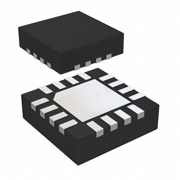
- Part No.:
- STSPIN250
- Manufacturer:
- STMicroelectronics
- Category:
- Motor Drivers, Controllers
- Package:
- 16-VFQFN Exposed Pad
- Datasheet:
-
 STSPIN250.pdf
- Description:
- IC MOTOR DRIVER 0V-5V 16VFQFPN
- Quantity:
- Payment:

- Shipping:

Inventory:12,365
Please send an inquiry. Send us your inquiry, and we will respond immediately.
Product details
Overview
STSPIN250 from STMicroelectronics is a low-voltage brush DC motor driver IC integrating a fully protected full-bridge power stage with PWM current control, 1.8–10 V supply range, 2.6 Arms continuous output (with OUTAx paralleled to OUTBx), 0.2 Ω typ. total RDS(ON), and <80 nA standby current - used in battery-powered portable medical devices, shavers, and robotics.
For engineers reviewing the STSPIN250 datasheet, STSPIN250 pinout, STSPIN250 application, or STSPIN250 equivalent, this page delivers verified technical context, validated pin functions, real-world use cases, and confirmed alternative options for low-power DC motor control designs.
Technical Context
The STSPIN250 implements a fixed OFF-time PWM current controller where VSENSE is compared against an external reference voltage applied at REF; when threshold exceeded, the bridge enters slow-decay mode via simultaneous low-side activation. The OFF time is externally programmable via ROFF (10–150 µs range) with RC stabilization per Table 10.
It features non-dissipative overcurrent protection per output, thermal shutdown at 160 °C with 40 °C hysteresis, and short-circuit detection across all fault modes (to GND, VS, or inter-output). EN\FAULT serves dual role: enable input and open-drain fault indicator that discharges CEN upon trip.
Key Specifications
| Parameter | Value and Actual Design Meaning |
|---|---|
| Supply Voltage Range | 1.8 V to 10 V - supports single-cell Li-ion, NiMH, and alkaline battery systems without external regulation. |
| Continuous Output Current | 2.6 Arms - achievable only when OUTAx and OUTBx are paralleled per datasheet configuration (Table 5). |
| Total RDS(ON) | 0.2 Ω typ. (HS + LS) at VS = 10 V, IOUT = 1.3 A - enables high-efficiency operation with minimal conduction loss. |
| Standby Current | <80 nA - achieved by forcing STBY\RESET low, cutting control circuitry supply and placing outputs in high-Z. |
| Current Sense Threshold Accuracy | ±15 mV offset on VSENSE - directly impacts peak current error; requires careful PCB layout and REF filtering. |
| Thermal Shutdown Threshold | 160 °C with 40 °C hysteresis - prevents latch-up during sustained overload; recovery occurs only after junction cools below 120 °C. |
| ESD Robustness | HBM Class H2 (2 kV), CDM Class C2a (500 V) - meets industrial handling requirements without additional protection circuitry. |
Pinout & Package
STSPIN250 is housed in a thermally enhanced VFQFPN 3 × 3 × 1.0 mm, 16-lead package with exposed pad (EPAD) for improved heat dissipation. The package complies with ECOPACK® environmental standards and uses fine-pitch (0.5 mm) leads.
| Pin/Terminal | Circuit Role | Design Meaning |
|---|---|---|
| PH | Logic input | Phase control signal determining motor direction; interpreted with PWM to define full-bridge state (Table 8). |
| PWM | Logic input | Switching control input; combined with PH to generate ON/OFF states and trigger current limiting cycle. |
| OUTA1 / OUTB1 | Power output | Must be connected together to form one half-bridge leg; drives motor terminal A when paralleled. |
| OUTA2 / OUTB2 | Power output | Must be connected together to form second half-bridge leg; drives motor terminal B when paralleled. |
| SENSEA / SENSEB | Power output | Current sense nodes; tied together and connected to shunt resistor; feed internal comparator for current regulation. |
| REF | Analog input | Reference voltage (0.1–0.5 V) setting peak motor current via ILOAD,peak = VREF/RSNS. |
| TOFF | Analog input | External resistor (ROFF) sets OFF time (10–150 µs); RC network (RRCOFF/CRCOFF) required for stability. |
| EN\FAULT | Logic input / open-drain output | Active-low enable; fault indicator pulls low during overcurrent/thermal events, discharging external CEN capacitor. |
| STBY\RESET | Logic input | Active-low entry into ultra-low-power mode (<80 nA); disables power stage and cuts internal bias supplies. |
| VS | Supply | Main motor supply input (1.8–10 V); powers both power stage and logic; decoupled with CS and CSPOL capacitors. |
| GND / EPAD | Ground | Primary ground return and thermal path; EPAD must be soldered to PCB ground plane per Figure 16 footprint. |
| TEST0 / TEST1 | Reserved | No internal connection; must be tied to GND per datasheet requirement (Figure 2 note). |
Key Features
| Feature | Design Value |
|---|---|
| Programmable fixed OFF-time current control | Enables precise peak current regulation independent of supply or temperature drift; ROFF adjusts decay duration from 10 to 150 µs. |
| Non-dissipative overcurrent protection | Detects overloads without shunt resistor heating; triggers immediate bridge disable and EN\FAULT assertion without energy dump into sense resistor. |
| Zero-consumption standby mode | Reduces system quiescent draw to <80 nA by gating internal regulators - extends battery life in intermittent-use applications like toothbrushes. |
| Integrated thermal shutdown with hysteresis | Shuts down at 160 °C and remains off until junction cools to 120 °C, preventing cycling during marginal thermal conditions. |
| Short-circuit protection coverage | Monitors all failure modes: output-to-GND, output-to-VS, and inter-output shorts - critical for unattended portable equipment safety. |
Applications
| Portable Medical Devices | Personal Care Appliances |
|---|---|
|
Use Scenario: Battery-powered insulin pumps and handheld diagnostic tools requiring silent, reliable motor actuation over multi-day cycles. IC Role / Device Role / Timing Role: Full-bridge motor driver with current-regulated commutation and ultra-low standby leakage. Use Value: Enables >14-day battery life using single AA cell due to <80 nA standby current and efficient 0.2 Ω RDS(ON). |
Use Scenario: Rechargeable electric toothbrushes and sonic facial cleansers needing bidirectional, variable-speed motor control. IC Role / Device Role / Timing Role: Directional (PH) and speed (PWM)-controlled DC driver with integrated current limiting and thermal foldback. Use Value: Eliminates need for external current-sense amplifier and discrete protection FETs - reduces BOM count by 4 components. |
| POS Printers & Scanners | Educational Robotics Kits |
|
Use Scenario: Compact thermal receipt printers and barcode scanners powered by USB or coin cells, demanding low EMI and fast wake-up. IC Role / Device Role / Timing Role: Low-voltage motor driver with fast EN propagation delay (55 ns) and noise-immune sense architecture. Use Value: Achieves <100 µs wake-from-standby response while maintaining <15 mV sense offset - ensures accurate low-current positioning. |
Use Scenario: Entry-level STEM robotics platforms using 3–6 V alkaline or LiPo batteries, requiring robust fault handling for student misuse. IC Role / Device Role / Timing Role: Fault-tolerant motor driver with auto-recovering EN\FAULT signaling and short-circuit detection on all output paths. Use Value: Survives accidental motor stall or wiring shorts without damage - reduces field returns in classroom deployments. |
Equivalent & Alternatives
The following parts are listed as comparable options for similar low-voltage brushed DC motor driver applications.
| Alternative Part | Technical Difference | Application Difference | Selection Advice |
|---|---|---|---|
| TB67H420FNG | Higher voltage range (4.5–44 V), 3.0 Arms, no standby mode, larger HTSSOP-28 package. | Requires external current sense and thermal monitoring; unsuitable for sub-2 V battery operation. | Select when driving higher-voltage motors (>12 V) and board space allows larger footprint. |
| DRV8876N | 1.65–11 V supply, 3.6 Arms, 0.12 Ω RDS(ON), but 2.5 µA standby current - 31× higher than STSPIN250. | Lacks ultra-low-power standby; not viable for multi-week battery life targets in portable healthcare. | Prefer for high-current, short-duty-cycle applications where efficiency matters more than quiescent drain. |
Compared with TB67H420FNG and DRV8876N, STSPIN250 uniquely delivers sub-80 nA standby consumption and integrated non-dissipative overcurrent protection in a 3 × 3 mm VFQFPN - making it the only option qualified for multi-month battery life in wearable and handheld medical devices.
Availability
STSPIN250 is available at Aetrix Electronics and suitable for portable medical devices, personal care appliances, POS printers, and educational robotics requiring stable component supply, long-lifecycle support, and RoHS-compliant packaging.
Supply support for STSPIN250 includes scheduled delivery planning, volume procurement assistance, BOM continuity management, traceable sourcing, and lifecycle availability coordination for OEM customers, industrial embedded developers, connected-device designers, and electronics production programs.
Manufacturer
STMicroelectronics is a global semiconductor leader headquartered in Geneva, Switzerland, designing and manufacturing microcontrollers, power ICs, sensors, and analog solutions for industrial, automotive, and consumer markets.
The STSPIN family targets compact, battery-efficient motion control - specifically engineered for space-constrained, low-voltage brushed DC applications where integration, protection, and ultra-low quiescent power are mandatory.
FAQ
What is the minimum supply voltage required for STSPIN250 to operate correctly?
The STSPIN250 has a guaranteed turn-on threshold of 1.45 V (typ. 1.65 V) and operates down to 1.8 V per recommended conditions. Below 1.8 V, timing margins shrink and current regulation accuracy degrades; operation below 1.45 V is not functional. It is validated for single-cell NiMH (1.2 V nominal) only if peak discharge stays above 1.45 V.
How does the STSPIN250 implement non-dissipative overcurrent protection?
When sensed current exceeds the threshold (2 A per output or 4 A with paralleled outputs), the device disables the power stage and asserts EN\FAULT low via an internal open-drain MOSFET - sinking external CEN charge without dissipating energy in the sense resistor. Recovery requires CEN to recharge through REN past VRELEASE (≤0.4 V).
Can STSPIN250 drive a motor in both directions with only two control signals?
Yes - direction is controlled by the PH input and speed by PWM, per the truth table (Table 8). With EN\FAULT high, PH = 0 and PWM = 1 drives current from X1 to X2; PH = 1 and PWM = 1 reverses flow from X1 to X2. Both outputs go to high-Z when EN\FAULT is low.
What is the purpose of the TEST0 and TEST1 pins on STSPIN250?
TEST0 and TEST1 are reserved, unconnected die test pads. Per datasheet Figure 2 note and Table 6, they must be externally tied to GND on the PCB - floating or biased connections may cause undefined behavior or reduced ESD robustness. No functionality is assigned to them in production operation.
STSPIN250 Specifications
- Product attributes
- Attribute value
- Manufacturer:
- STMicroelectronics
- Series:
- STSPIN2
- Package/Case:
- 16-VFQFN Exposed Pad
- Packaging:
- Tape & Reel (TR)
- Product Status:
- Active
- Motor Type - Stepper:
- -
- Motor Type - AC, DC:
- Brushed DC
- Function:
- Driver - Fully Integrated, Control and Power Stage
- Output Configuration:
- Half Bridge (4)
- Interface:
- PWM
- Technology:
- Power MOSFET
- Step Resolution:
- -
- Applications:
- General Purpose
- Current - Output:
- 2.6A
- Voltage - Supply:
- 0V ~ 5V
- Voltage - Load:
- 1.8V ~ 10V
- Operating Temperature:
- -40°C ~ 150°C (TJ)
- Grade:
- -
- Qualification:
- -
- Mounting Type:
- Surface Mount
- Supplier Device Package:
- 16-VFQFPN (3x3)
STSPIN250 FAQ
1.How can I place an order for STSPIN250 through Aetrix?
Please submit a Request for Quotation (RFQ) for STSPIN250 on Aetrix. Our sales agent will provide a competitive quotation and guide you through the order confirmation once you accept the terms.
2.Are the price and stock information for STSPIN250 reliable?
The price and inventory of STSPIN250 are updated periodically and may fluctuate due to market conditions. Stock and pricing data are typically refreshed every 24 hours. Quotation validity for STSPIN250 is usually 5 days.
3.What payment methods are accepted for STSPIN250?
We accept Wire Transfer, PayPal, Credit Card, Western Union, MoneyGram, and Escrow for STSPIN250 transactions.
Note: Certain payment methods may incur a processing fee.
4.How is shipping managed for STSPIN250?
STSPIN250 orders can be shipped via leading logistics carriers, including DHL, UPS, FedEx, TNT, or Registered Mail.
Once your STSPIN250 order is processed, you will receive an email with the shipment details and tracking number.
Note: Tracking information may take up to 24 hours to appear. Express delivery typically takes 3–5 business days.
5.How can I obtain technical support or documentation for STSPIN250?
For technical support, including STSPIN250 datasheets, pinout diagrams, or application guidance, please contact our engineering support team. They can provide detailed documentation and assistance for your STSPIN250 requirements.
6.How does Aetrix verify that STSPIN250 is sourced from the original manufacturer or authorized distributors?
All STSPIN250 products on Aetrix are procured from qualified distributors and authorized channels. Our dedicated quality assurance team conducts strict verification, including traceability checks and, if necessary, third-party testing. This ensures that STSPIN250 meets industry standards.
7.What is the process for return or replacement of STSPIN250?
All STSPIN250 units undergo pre-shipment inspection (PSI). If there is an issue with STSPIN250, returns or replacements are accepted under the following conditions:
1.Quantity discrepancies, incorrect items, or visible external defects (such as breakage or corrosion), acknowledged by Aetrix.
2.The issue is reported within 90 days of delivery.
3.The STSPIN250 part is unused and in its original packaging.
Return procedure for STSPIN250:
1.Submit a request within 90 days.
2.Obtain a Return Material Authorization (RMA) from Aetrix.
STSPIN250 Tags

-
DRV2603RUNR
Texas Instruments

-
DRV8837CDSGR
Texas Instruments

-
DRV8837DSGR
Texas Instruments
-
DRV8838DSGR
Texas Instruments

-
DRV8839DSSR
Texas Instruments

-
EMC2301-1-ACZL-TR
Microchip Technology
-
DRV8231ADSGR
Texas Instruments

-
EMC2302-2-AIZL-TR
Microchip Technology

-
DRV8800PWPR
Texas Instruments
-
DRV8835DSSR
Texas Instruments

-
EMC2303-1-KP-TR
Microchip Technology

-
DRV8876PWPR
Texas Instruments
Tech Hub

A practical engineering and sourcing framework covering lifecycle verification, lifetime-buy calculations, replacement qualification, supplier checks and counterfeit-risk controls.

TTL and CMOS logic families differ in thresholds, loading, output drive, power and timing. This engineering guide compares 74HC and 74HCT, calculates noise margins and checks 3.3 V/5 V compatibility.

A practical engineering guide to 3.3V and 5V logic compatibility, input thresholds, resistor dividers, translator ICs, MOSFET level shifting, I2C pull-ups, timing limits and power-sequencing risks.

The 74HC595 uses push-pull logic outputs, while the TPIC6B595 uses 50 V open-drain DMOS sinks for higher-power loads. This guide compares timing, current limits, 3.3 V interfacing, load wiring, thermal…

The 74HC595 converts serial data into eight stable parallel outputs. This guide covers pin functions, shift and storage timing, OE and MR behavior, drive-current limits, cascading, voltage compatibilit…

A technical comparison of level-sensitive latches and edge-triggered flip-flops, covering timing windows, setup and hold limits, master–slave operation, time borrowing, race-through, HDL inference and…

A D latch stores one bit while Enable controls when data can pass. This reference covers gate-level operation, truth tables, transparency, setup and hold timing, LE versus OE, common ICs and practical …

An SR latch stores one bit through cross-coupled feedback. This engineering reference covers NOR and NAND implementations, truth tables, forbidden-state recovery, gated operation, switch debouncing, fa…

Latch circuits retain one bit through feedback. This technical reference covers SR and D latches, truth tables, transparency, timing limits, latch-versus-flip-flop behavior, applications and common log…

An engineering guide to LED driver operation, constant-current and constant-voltage outputs, linear and switching topologies, dimming, IC selection, calculations, replacement compatibility, and fault c…


