
 My Inquiry
 My Account


STMicroelectronics STULPI01BTBR
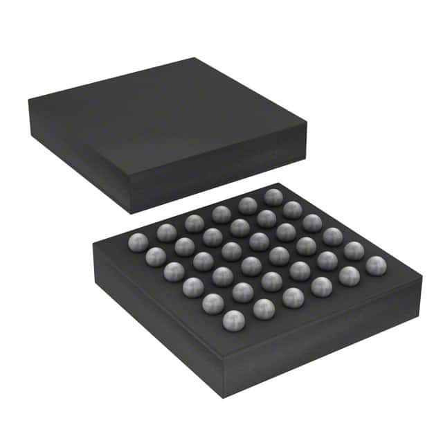
- Part No.:
- STULPI01BTBR
- Manufacturer:
- STMicroelectronics
- Category:
- Drivers, Receivers, Transceivers
- Package:
- 36-TFBGA
- Datasheet:
-
 STULPI01BTBR.pdf
- Description:
- IC TRANSCEIVER 1/1 36TFBGA
- Quantity:
- Payment:

- Shipping:

Inventory:10,983
Please send an inquiry. Send us your inquiry, and we will respond immediately.
Product details
Overview
STULPI01BTBR from STMicroelectronics is a high-speed USB 2.0 On-The-Go (OTG) ULPI transceiver in µTFBGA36 package, providing full PHY layer compliance with USB 2.0, OTG Supplement 1.0a, and ULPI Specification 1.1. It supports 480 Mbit/s High-speed, 12 Mbit/s Full-speed, and 1.5 Mbit/s Low-speed modes, integrates dual LDOs (3.3 V and 1.2 V), and enables SRP/HNP for dual-role operation in mobile battery-powered systems.
For engineers reviewing the STULPI01BTBR datasheet, STULPI01BTBR pinout, STULPI01BTBR application, or STULPI01BTBR equivalent, this transceiver is selected for low-power USB OTG interface design where ULPI bus timing, VBUS/ID detection accuracy, integrated termination, and power-down current <2 µA are critical selection criteria.
Technical Context
The device implements a complete USB 2.0 PHY with differential drivers/receivers for DP/DM, on-die VBUS comparators (4.4–4.75 V valid threshold), ID line detector (70 µA pull-up, 1 kΩ GND/100 kΩ FLOAT detection), and ULPI wrapper supporting synchronous 12-pin register-mapped control. Its oscillator input (XI) requires an external 19.2 or 26 MHz square wave clock with VDVIO amplitude and ≥4 ns edge rate.
Power management includes dedicated pins for power-down (CSn/PWRDN), reset (RESETn active-low), and external charge pump control (PSWn open-drain), alongside integrated overcurrent detection via VB_REF_FAULT with 20–95 mV trip threshold referenced to VBUS. The internal 1.2 V and 3.3 V regulators supply core logic and analog blocks independently.
Key Specifications
| Parameter | Value and Actual Design Meaning |
|---|---|
| USB Speed Modes | 480 Mbit/s HS, 12 Mbit/s FS, 1.5 Mbit/s LS - enables full backward compatibility and high-bandwidth peripheral attachment |
| ULPI Compliance | Fully compliant with ULPI 1.1 register map and timing - ensures interoperability with UTMI+-based host/device ASICs |
| Supply Range | +3.0 V to +4.5 V VBAT - matches single-cell Li-ion/Li-poly battery systems without external regulation |
| Power-Down Current | 0.4–2 µA - extends battery life in suspend/idle states for portable OTG devices |
| VBUS Valid Threshold | 4.4–4.75 V - meets USB 2.0 specification for reliable host negotiation and session detection |
| ID Detection Logic | Distinguishes ID_GND (≤1 kΩ) vs ID_FLOAT (≥100 kΩ) - determines initial A/B device role per OTG standard |
| UART Mode Support | 2.7 V operation with D0/D1 as TXD/RXD - provides fallback serial debug interface independent of USB stack |
Pinout & Package
STULPI01BTBR is housed in a 36-ball µTFBGA package (ball pitch: 0.5 mm, body size: 3.5 × 3.5 mm), optimized for space-constrained mobile applications. All digital I/O operate at VDVIO (1.65–3.6 V), while DP, DM, ID, VBUS, and VB_REF_FAULT are 5 V tolerant.
| Pin/Terminal | Circuit Role | Design Meaning |
|---|---|---|
| D0–D7 | ULPI bidirectional data bus | Carry register reads/writes and UART TXD/RXD (D0/D1); referenced to VDVIO |
| CLK, DIR, NXT, STP | ULPI control signals | Provide synchronous 60 MHz interface timing (CLK out), direction control, and handshaking |
| RESETn | Asynchronous active-low reset | Forces hardware initialization; must be held low ≥1 µs after power stabilization |
| CSn/PWRDN | Chip select / power-down enable | Active-high assertion enters ultra-low-power mode (<2 µA); overrides all other states |
| DP / DM | USB 2.0 differential data pair | 5 V tolerant; include integrated HS termination and FS/LS pull-up/down resistors |
| ID | OTG role identification input | Reads connector ID state to determine A-device (host) or B-device (peripheral) at startup |
| VBUS | USB power bus monitor | Input with 40–100 kΩ impedance; feeds comparator for session valid (4.4–4.75 V) and overcurrent detection |
| VB_REF_FAULT | Overcurrent reference input | Accepts external OC signal or internal reference; trip window: 20–95 mV below VBUS |
| PSWn | External charge pump control | Open-drain output enabling higher VBUS sourcing capability beyond standard 500 mA |
| XI | External clock input | Accepts 19.2/26 MHz square wave; hysteresis ≥500 mV ensures noise immunity |
| 3V3V / 1V2V | Internal LDO outputs | Stable regulated supplies for analog/digital blocks; require local 1.5 µF bypassing |
| VDVIO | Digital I/O supply | Separate rail for ULPI interface; decoupling required per ball (100 nF–1 µF) |
Key Features
| Feature | Design Value |
|---|---|
| Integrated dual-LDO regulation | On-chip 3.3 V and 1.2 V supplies eliminate need for external regulators in compact designs |
| ULPI 1.1 register-compliant interface | Full 12-pin synchronous interface with standardized register map (0x00–0x1F) for seamless ASIC integration |
| OTG protocol support | Hardware-accelerated Session Request Protocol (SRP) and Host Negotiation Protocol (HNP) reduce firmware overhead |
| USB 2.0 short-circuit withstand | Built-in protection survives DP/DM shorts to VBUS/GND without latch-up or damage |
| Multi-mode power management | Five defined low-power states (Suspend, UART, Power-down, VIO OFF, Sleep) with sub-µA quiescent current |
| 5 V tolerant I/O on critical pins | DP, DM, ID, VBUS, VB_REF_FAULT tolerate up to 5.5 V - simplifies level-shifting and ESD protection |
Applications
| Smartphone OTG Adapter | Portable Media Player |
|---|---|
|
Use Scenario: Enables USB flash drive or keyboard connection to Android smartphones via micro-AB receptacle. IC Role / Device Role / Timing Role: Acts as OTG PHY, detecting ID pin to initiate A-device (host) mode and managing VBUS negotiation using SRP/HNP. Use Value: Delivers 480 Mbit/s throughput with <2 µA power-down current, extending battery runtime during accessory use. |
Use Scenario: Connects MP3 player to PC for firmware updates and media sync via USB cable. IC Role / Device Role / Timing Role: Serves as USB device PHY, providing FS/LS signaling and integrated pull-up resistors for enumeration. Use Value: Eliminates external 1.5 kΩ DP pull-up and 3.3 V regulator, reducing BOM count by two components. |
| Digital Still Camera | Portable Navigation Device |
|
Use Scenario: Allows direct photo transfer to USB printer or mass storage without host PC. IC Role / Device Role / Timing Role: Functions as dual-role OTG transceiver, switching between peripheral (when connected to PC) and host (when connected to printer). Use Value: Integrated HS termination and eye-diagram-compliant drivers ensure reliable 480 Mbit/s transfers across varying cable lengths. |
Use Scenario: Supports USB tethering to smartphone for internet access and GPS data logging to USB memory stick. IC Role / Device Role / Timing Role: Provides robust VBUS monitoring and overcurrent detection to protect against faulty cables or chargers. Use Value: VB_REF_FAULT input enables precise 20–95 mV OC threshold setting, improving safety margin over discrete solutions. |
Equivalent & Alternatives
The following parts are listed as comparable options for similar USB OTG transceiver applications.
| Alternative Part | Technical Difference | Application Difference | Selection Advice |
|---|---|---|---|
| ISP1504HN | Single 3.3 V supply only; no integrated 1.2 V LDO; requires external 3.3 V regulator | Lacks UART mode and VBAT direct support; less suitable for battery-only systems | Prefer when system already provides clean 3.3 V and UART debug is unnecessary |
| USB3320C-EZK | Supports USB 2.0 + ULPI but adds USB 3.0 SS capability; larger QFN48 package | Higher pin count and cost; over-specified for pure USB 2.0 OTG use cases | Choose only if future USB 3.0 upgrade path or additional HS PHY channels are required |
Compared with ISP1504HN and USB3320C-EZK, STULPI01BTBR uniquely combines single-battery-input operation, integrated dual-LDOs, UART fallback mode, and µTFBGA36 footprint-making it optimal for cost- and space-sensitive mobile OTG endpoints where power efficiency and minimal external components are mandatory.
Availability
STULPI01BTBR is available at Aetrix Electronics and suitable for smartphone OTG adapters, portable media players, digital still cameras, and portable navigation devices requiring stable component supply across long production lifecycles.
Supply support for STULPI01BTBR includes scheduled delivery planning, volume procurement assistance, BOM continuity management, traceable sourcing, and lifecycle availability coordination for OEM customers, industrial embedded developers, connected-device designers, and electronics production programs.
Manufacturer
STMicroelectronics is a global semiconductor leader headquartered in Geneva, Switzerland, designing and manufacturing microcontrollers, analog ICs, MEMS, and power management solutions for automotive, industrial, and consumer markets.
STULPI01BTBR belongs to ST's USB Physical Layer product line, engineered specifically for low-power, small-footprint USB 2.0 OTG implementations in battery-operated handheld devices where ULPI interface compatibility and integrated regulation are essential.
FAQ
What external components are mandatory for STULPI01BTBR operation?
Mandatory external components include: a 4.7 µF tank capacitor (CT) on VBUS, a 12 kΩ ±1% reference resistor (RREF) for overcurrent detection, and local bypass capacitors - 1 µF on VBAT, 1.5 µF on 3V3V, 1.5 µF on 1V2V, and 100 nF–1 µF on each VDVIO ball. No crystal is needed; XI accepts only external square-wave clock.
How does STULPI01BTBR handle USB host/peripheral role switching?
Role switching is managed via hardware-supported Session Request Protocol (SRP) and Host Negotiation Protocol (HNP). The ID pin detects physical connector type at startup to set initial role; subsequent HNP requests trigger controlled handover between A-device (host) and B-device (peripheral) without software reset or bus re-enumeration.
Can STULPI01BTBR operate without an external clock source?
No. STULPI01BTBR requires an external 19.2 MHz or 26 MHz square-wave clock applied to the XI pin. XO must be left floating or grounded; crystal oscillators are not supported. Clock rise/fall times must be ≤4 ns to meet ULPI timing requirements and avoid metastability in the CLK domain.
What is the function of the PSWn pin and how is it used in practice?
PSWn is an open-drain output that controls an external charge pump to boost VBUS sourcing capability beyond the standard 500 mA limit. When asserted low, it enables the pump to deliver higher currents for powering USB peripherals like HDDs or hubs - critical in portable host applications where wall adapters are unavailable.
STULPI01BTBR Specifications
- Product attributes
- Attribute value
- Manufacturer:
- STMicroelectronics
- Series:
- -
- Package/Case:
- 36-TFBGA
- Packaging:
- Tape & Reel (TR)
- Product Status:
- Active
- Type:
- Transceiver
- Protocol:
- -
- Number of Drivers/Receivers:
- 1/1
- Duplex:
- -
- Receiver Hysteresis:
- -
- Data Rate:
- -
- Voltage - Supply:
- 3V ~ 4.5V
- Operating Temperature:
- -40°C ~ 85°C
- Grade:
- -
- Qualification:
- -
- Mounting Type:
- Surface Mount
- Supplier Device Package:
- 36-TFBGA (3.5x3.5)
STULPI01BTBR FAQ
1.How can I place an order for STULPI01BTBR through Aetrix?
Please submit a Request for Quotation (RFQ) for STULPI01BTBR on Aetrix. Our sales agent will provide a competitive quotation and guide you through the order confirmation once you accept the terms.
2.Are the price and stock information for STULPI01BTBR reliable?
The price and inventory of STULPI01BTBR are updated periodically and may fluctuate due to market conditions. Stock and pricing data are typically refreshed every 24 hours. Quotation validity for STULPI01BTBR is usually 5 days.
3.What payment methods are accepted for STULPI01BTBR?
We accept Wire Transfer, PayPal, Credit Card, Western Union, MoneyGram, and Escrow for STULPI01BTBR transactions.
Note: Certain payment methods may incur a processing fee.
4.How is shipping managed for STULPI01BTBR?
STULPI01BTBR orders can be shipped via leading logistics carriers, including DHL, UPS, FedEx, TNT, or Registered Mail.
Once your STULPI01BTBR order is processed, you will receive an email with the shipment details and tracking number.
Note: Tracking information may take up to 24 hours to appear. Express delivery typically takes 3–5 business days.
5.How can I obtain technical support or documentation for STULPI01BTBR?
For technical support, including STULPI01BTBR datasheets, pinout diagrams, or application guidance, please contact our engineering support team. They can provide detailed documentation and assistance for your STULPI01BTBR requirements.
6.How does Aetrix verify that STULPI01BTBR is sourced from the original manufacturer or authorized distributors?
All STULPI01BTBR products on Aetrix are procured from qualified distributors and authorized channels. Our dedicated quality assurance team conducts strict verification, including traceability checks and, if necessary, third-party testing. This ensures that STULPI01BTBR meets industry standards.
7.What is the process for return or replacement of STULPI01BTBR?
All STULPI01BTBR units undergo pre-shipment inspection (PSI). If there is an issue with STULPI01BTBR, returns or replacements are accepted under the following conditions:
1.Quantity discrepancies, incorrect items, or visible external defects (such as breakage or corrosion), acknowledged by Aetrix.
2.The issue is reported within 90 days of delivery.
3.The STULPI01BTBR part is unused and in its original packaging.
Return procedure for STULPI01BTBR:
1.Submit a request within 90 days.
2.Obtain a Return Material Authorization (RMA) from Aetrix.
STULPI01BTBR Tags

-
ATA6561-GAQW-N
Microchip Technology
-
ATA6561-GBQW-N
Microchip Technology

-
AM26LS32ACDR
Texas Instruments

-
SP485CN-L/TR
MaxLinear, Inc.
-
SP485EN-L/TR
MaxLinear, Inc.
-
SP485EEN-L/TR
MaxLinear, Inc.
-
SP485ECN-L/TR
MaxLinear, Inc.
-
THVD1400DR
Texas Instruments
-
AM26C31IDR
Texas Instruments

-
TLIN1021ADRQ1
Texas Instruments
-
MAX232IDR
Texas Instruments
-
AM26C32IDR
Texas Instruments
Tech Hub

A practical engineering and sourcing framework covering lifecycle verification, lifetime-buy calculations, replacement qualification, supplier checks and counterfeit-risk controls.

TTL and CMOS logic families differ in thresholds, loading, output drive, power and timing. This engineering guide compares 74HC and 74HCT, calculates noise margins and checks 3.3 V/5 V compatibility.

A practical engineering guide to 3.3V and 5V logic compatibility, input thresholds, resistor dividers, translator ICs, MOSFET level shifting, I2C pull-ups, timing limits and power-sequencing risks.

The 74HC595 uses push-pull logic outputs, while the TPIC6B595 uses 50 V open-drain DMOS sinks for higher-power loads. This guide compares timing, current limits, 3.3 V interfacing, load wiring, thermal…

The 74HC595 converts serial data into eight stable parallel outputs. This guide covers pin functions, shift and storage timing, OE and MR behavior, drive-current limits, cascading, voltage compatibilit…

A technical comparison of level-sensitive latches and edge-triggered flip-flops, covering timing windows, setup and hold limits, master–slave operation, time borrowing, race-through, HDL inference and…

A D latch stores one bit while Enable controls when data can pass. This reference covers gate-level operation, truth tables, transparency, setup and hold timing, LE versus OE, common ICs and practical …

An SR latch stores one bit through cross-coupled feedback. This engineering reference covers NOR and NAND implementations, truth tables, forbidden-state recovery, gated operation, switch debouncing, fa…

Latch circuits retain one bit through feedback. This technical reference covers SR and D latches, truth tables, transparency, timing limits, latch-versus-flip-flop behavior, applications and common log…

An engineering guide to LED driver operation, constant-current and constant-voltage outputs, linear and switching topologies, dimming, IC selection, calculations, replacement compatibility, and fault c…


