
 My Inquiry
 My Account


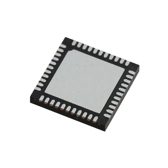
STMicroelectronics STW82103B
- Part No.:
- STW82103B
- Manufacturer:
- STMicroelectronics
- Category:
- RF Mixers
- Package:
- 44-VFQFN Exposed Pad
- Datasheet:
-
 STW82103B.pdf
- Description:
- IC MIXER 2.3-2.7GHZ DWN CONV
- Quantity:
- Payment:

- Shipping:

Inventory:3,747
Please send an inquiry. Send us your inquiry, and we will respond immediately.
Product details
Overview
STW82103B from STMicroelectronics is a highly integrated RF down converter with embedded integer-N synthesizer, designed for cellular infrastructure receivers and digital PA linearization loops. It delivers 8 dB conversion gain, 10.5 dB noise figure, +25 dBm IIP3 linearity, and operates across 2300–2700 MHz RF and 70–400 MHz IF bands.
For engineers reviewing the STW82103B datasheet, STW82103B pinout, STW82103B application, or STW82103B equivalent, key selection criteria include dual VCO auto-calibration (LOA: 2200–2550 MHz, LOB: 2500–3000 MHz), dual digital interface (SPI/I²C), integrated DAC for PIN diode control, and 44-pin VFQFPN package with exposed thermal pad.
Technical Context
The STW82103B integrates a passive RF mixer, dual differential auto-calibrating VCOs, and an integer-N PLL with programmable prescaler (16/17 or 19/20), 10-bit reference divider, and adjustable charge pump current. Its RF balun enables direct 50 Ω single-ended RF input, while the IF amplifier drives 200 Ω filters.
The device implements two independent VCO calibration paths (VCOA/VCOB), digital lock detection, mute-until-lock functionality, and supports both standard and diversity modes-enabling simultaneous dual-LO operation with fast 150 µs lock time and excellent integrated phase noise performance.
Key Specifications
| Parameter | Value and Actual Design Meaning |
|---|---|
| RF Frequency Range | 2300–2700 MHz: Covers LTE Band 7, 38, 40, and 41 for cellular infrastructure front-ends. |
| IF Output Range | 70–400 MHz: Supports baseband sampling and IF filtering in zero-IF and low-IF receiver architectures. |
| IIP3 | +25 dBm: Enables high dynamic range reception in dense multi-carrier environments without external pre-distortion. |
| Noise Figure | 10.5 dB: Optimized for sensitivity-critical receive paths in macro and small-cell base stations. |
| Conversion Gain | 8 dB: Reduces need for external IF amplification stages, simplifying signal chain design. |
| VCO Calibration | Auto-centering for LOA (2200–2550 MHz) and LOB (2500–3000 MHz): Eliminates manual tuning and improves production yield. |
| Synthesizer Lock Time | 150 µs: Meets fast frequency-hopping requirements in TDD-LTE and dynamic spectrum allocation systems. |
| Dual Bus Interface | SPI and I²C (fast mode) with 3-bit address (1101A2A1A0): Enables flexible host controller integration in mixed-signal SoC platforms. |
Pinout & Package
STW82103B is housed in a 44-lead VFQFPN package (7 × 7 × 1.0 mm) with exposed thermal pad for enhanced RF thermal management and EMI shielding. The package supports reflow soldering per JEDEC J-STD-020 and is rated for -40 °C to +85 °C ambient operation.
| Pin/Terminal | Circuit Role | Design Meaning |
|---|---|---|
| RF_IN (Pin 38) | RF signal input | Single-ended 50 Ω interface via integrated balun; no external matching required. |
| IF_OUTP / IF_OUTN (Pins 31–32) | Differential IF output | Open-collector outputs compatible with 200 Ω differential filter inputs at 5 V supply. |
| OUTBUFP / OUTBUFN (Pins 16–17) | Differential LO buffer output | Drives external mixers or quadrature modulators; open-collector @ 3.3 V. |
| I_PINDRV1 / I_PINDRV2 (Pins 43–44) | DAC current outputs | Programmable dual-current sink for driving external PIN diode attenuators in AGC loops. |
| REF_CLK (Pin 23) | Reference clock input | Accepts 10–100 MHz CMOS-level reference; internal buffer supports wide frequency range. |
| LOCK_DET (Pin 22) | Digital lock status indicator | CMOS output asserts high when PLL achieves frequency and phase lock. |
| DBUS_SEL (Pin 25) | Interface mode select | High = SPI; Low = I²C - enables runtime bus switching without hardware change. |
Key Features
| Feature | Design Value |
|---|---|
| Integrated RF balun with internal matching | Enables direct 50 Ω single-ended RF connection, eliminating discrete baluns and matching networks. |
| Dual auto-calibrating VCOs (LOA/LOB) | Reduces system-level calibration effort and improves LO stability over temperature and process variation. |
| Embedded dual-output DAC | Replaces external DAC + op-amp + current buffers for PIN diode attenuation control in closed-loop ALC circuits. |
| Mute-until-lock function | Prevents spurious IF output during PLL acquisition, avoiding corruption of ADC sampling windows. |
| Supply flexibility | Separate 3.3 V analog/digital rails and 5 V analog rail (VDD_MIXDRV, VDD_IFAMP) optimize noise isolation and headroom. |
| Fast-mode I²C + SPI support | Allows seamless integration into FPGA-based control planes or microcontroller-based baseband processors. |
Applications
| Cellular Base Station Receiver | Digital Pre-Distortion Loop |
|---|---|
Use Scenario: Down-conversion of 2600 MHz LTE signals to 122.88 MHz IF for digitization in macrocell BTS. IC Role / Device Role / Timing Role: Primary RF-to-IF converter with integrated LO synthesis and automatic VCO centering. Use Value: Eliminates discrete VCO, loop filter, and IF amplifier stages, reducing BOM count by ≥7 components and PCB area by >35%. | Use Scenario: Feedback path in DPD-enabled remote radio head (RRH), capturing PA output for real-time correction. IC Role / Device Role / Timing Role: High-linearity IF sampling front-end with calibrated LO generation synchronized to transmit path. Use Value: +25 dBm IIP3 ensures accurate capture of distortion products up to 40 dB below carrier, enabling precise inverse modeling. |
| Small Cell Diversity Receiver | TDD-LTE Fast-Hopping Receiver |
Use Scenario: Dual-antenna diversity architecture using LOA and LOB simultaneously for independent RF paths. IC Role / Device Role / Timing Role: Dual-VCO diversity down converter supporting asynchronous LO frequencies (e.g., 2350 MHz and 2650 MHz). Use Value: On-chip VCO calibration eliminates inter-channel LO drift, maintaining >35 dB image rejection across temperature. | Use Scenario: Dynamic channel switching in TDD-LTE base station requiring sub-200 µs frequency reconfiguration. IC Role / Device Role / Timing Role: Synthesizer-controlled down converter with 150 µs lock time and digital lock detect for deterministic timing. Use Value: Guarantees clean IF output within 150 µs after frequency command, meeting 3GPP TS 36.104 timing constraints. |
Equivalent & Alternatives
The following parts are listed as comparable options for similar RF down converter with integrated synthesizer applications.
| Alternative Part | Technical Difference | Application Difference | Selection Advice |
|---|---|---|---|
| ADRF6612ACPZ-R7 | Higher NF (9.5 dB), wider RF range (700–2700 MHz), but no integrated DAC for PIN diode control. | Lacks on-chip DAC outputs; requires external current source for AGC, increasing component count. | Select when lower noise figure is critical and external DAC implementation is acceptable. |
| MAX2112ETM+ | Lower IIP3 (+19 dBm), fixed 2.1 GHz LO range, no dual-VCO architecture or auto-calibration. | Not suitable for multi-band diversity or wide-tuning applications; limited to narrowband FDD systems. | Select only for cost-sensitive, single-band FDD infrastructure where calibration overhead is managed externally. |
Compared with ADRF6612 and MAX2112, the STW82103B uniquely combines dual auto-calibrating VCOs, integrated DAC for analog loop control, and 150 µs lock time-making it optimal for compact, multi-standard, and fast-hopping cellular infrastructure designs.
Availability
STW82103B is available at Aetrix Electronics and suitable for cellular base station receivers, digital PA linearization loops, small cell diversity front-ends, and TDD-LTE fast-hopping systems requiring stable component supply and long-term manufacturability.
Supply support for STW82103B includes scheduled delivery planning, volume procurement assistance, BOM continuity management, traceable sourcing, and lifecycle availability coordination for OEM customers, industrial embedded developers, connected-device designers, and electronics production programs.
Manufacturer
STMicroelectronics is a global semiconductor leader headquartered in Geneva, specializing in analog, power, and RF solutions for automotive, industrial, and communications markets.
The STW82103B belongs to ST's RF transceiver IC product line, engineered specifically for high-performance, space-constrained cellular infrastructure equipment demanding integration, linearity, and rapid frequency agility.
FAQ
What is the recommended power-up sequence for STW82103B?
Apply AVCC1 (3.3 V analog), AVCC2 (5 V analog), and DVCC (3.3 V digital) simultaneously or in any order - no strict sequencing is required. However, REF_CLK must be stable before issuing configuration commands via SPI or I²C. VCO calibration should be initiated after power stabilization and before enabling RF path.
Does STW82103B support external VCO injection?
Yes - pins EXTVCO_INP (Pin 6) and EXTVCO_INN (Pin 5) accept differential external LO signals in External VCO Mode. This bypasses internal VCOs and allows use of higher-power or ultra-low-phase-noise external oscillators, with full synthesizer control retained for frequency programming.
How is the DAC output current programmed?
The dual DAC outputs (I_PINDRV1/I_PINDRV2) are controlled via register bits in the SPI/I²C interface. Each output supports 32 discrete current levels (0–1.2 mA typical), set independently through dedicated DAC control registers (DAC1_CTRL and DAC2_CTRL), enabling precise attenuation slope tuning in AGC loops.
Can STW82103B operate in diversity mode with different LO frequencies?
Yes - Diversity Master Mode supports independent programming of LOA and LOB frequencies (e.g., 2350 MHz and 2650 MHz), enabling true dual-path heterodyne down conversion. The device maintains separate calibration states and lock detection for each VCO, ensuring simultaneous stable operation without cross-talk.
STW82103B Specifications
- Product attributes
- Attribute value
- Manufacturer:
- STMicroelectronics
- Series:
- -
- Package/Case:
- 44-VFQFN Exposed Pad
- Packaging:
- Tray
- Product Status:
- Active
- RF Type:
- General Purpose
- Frequency:
- 2.3GHz ~ 2.7GHz
- Number of Mixers:
- 1
- Gain:
- 8.5dB
- Noise Figure:
- 10.5dB
- Secondary Attributes:
- Down Converter
- Current - Supply:
- 160mA
- Voltage - Supply:
- 3V ~ 5V
- Mounting Type:
- Surface Mount
- Supplier Device Package:
- 44-VFQFPN (7x7)
STW82103B FAQ
1.How can I place an order for STW82103B through Aetrix?
Please submit a Request for Quotation (RFQ) for STW82103B on Aetrix. Our sales agent will provide a competitive quotation and guide you through the order confirmation once you accept the terms.
2.Are the price and stock information for STW82103B reliable?
The price and inventory of STW82103B are updated periodically and may fluctuate due to market conditions. Stock and pricing data are typically refreshed every 24 hours. Quotation validity for STW82103B is usually 5 days.
3.What payment methods are accepted for STW82103B?
We accept Wire Transfer, PayPal, Credit Card, Western Union, MoneyGram, and Escrow for STW82103B transactions.
Note: Certain payment methods may incur a processing fee.
4.How is shipping managed for STW82103B?
STW82103B orders can be shipped via leading logistics carriers, including DHL, UPS, FedEx, TNT, or Registered Mail.
Once your STW82103B order is processed, you will receive an email with the shipment details and tracking number.
Note: Tracking information may take up to 24 hours to appear. Express delivery typically takes 3–5 business days.
5.How can I obtain technical support or documentation for STW82103B?
For technical support, including STW82103B datasheets, pinout diagrams, or application guidance, please contact our engineering support team. They can provide detailed documentation and assistance for your STW82103B requirements.
6.How does Aetrix verify that STW82103B is sourced from the original manufacturer or authorized distributors?
All STW82103B products on Aetrix are procured from qualified distributors and authorized channels. Our dedicated quality assurance team conducts strict verification, including traceability checks and, if necessary, third-party testing. This ensures that STW82103B meets industry standards.
7.What is the process for return or replacement of STW82103B?
All STW82103B units undergo pre-shipment inspection (PSI). If there is an issue with STW82103B, returns or replacements are accepted under the following conditions:
1.Quantity discrepancies, incorrect items, or visible external defects (such as breakage or corrosion), acknowledged by Aetrix.
2.The issue is reported within 90 days of delivery.
3.The STW82103B part is unused and in its original packaging.
Return procedure for STW82103B:
1.Submit a request within 90 days.
2.Obtain a Return Material Authorization (RMA) from Aetrix.
STW82103B Tags
-
MAX2671EUT+T
Analog Devices Inc./Maxim Integrated

-
ADEX-10+
Mini-Circuits
-
ADE-2+
Mini-Circuits
-
ADE-1+
Mini-Circuits
-
LT5560EDD#PBF
Analog Devices Inc.
-
LT5560EDD#TRPBF
Analog Devices Inc.

-
LTC5562IUC#TRPBF
Analog Devices Inc.
-
MAX2681EUT+T
Analog Devices Inc./Maxim Integrated
-
ADE-1ASK+
Mini-Circuits
-
ADE-1L+
Mini-Circuits
-
ADL5350ACPZ-R7
Analog Devices Inc.
-
AD608ARZ-RL
Analog Devices Inc.
Tech Hub

A practical engineering and sourcing framework covering lifecycle verification, lifetime-buy calculations, replacement qualification, supplier checks and counterfeit-risk controls.

TTL and CMOS logic families differ in thresholds, loading, output drive, power and timing. This engineering guide compares 74HC and 74HCT, calculates noise margins and checks 3.3 V/5 V compatibility.

A practical engineering guide to 3.3V and 5V logic compatibility, input thresholds, resistor dividers, translator ICs, MOSFET level shifting, I2C pull-ups, timing limits and power-sequencing risks.

The 74HC595 uses push-pull logic outputs, while the TPIC6B595 uses 50 V open-drain DMOS sinks for higher-power loads. This guide compares timing, current limits, 3.3 V interfacing, load wiring, thermal…

The 74HC595 converts serial data into eight stable parallel outputs. This guide covers pin functions, shift and storage timing, OE and MR behavior, drive-current limits, cascading, voltage compatibilit…

A technical comparison of level-sensitive latches and edge-triggered flip-flops, covering timing windows, setup and hold limits, master–slave operation, time borrowing, race-through, HDL inference and…

A D latch stores one bit while Enable controls when data can pass. This reference covers gate-level operation, truth tables, transparency, setup and hold timing, LE versus OE, common ICs and practical …

An SR latch stores one bit through cross-coupled feedback. This engineering reference covers NOR and NAND implementations, truth tables, forbidden-state recovery, gated operation, switch debouncing, fa…

Latch circuits retain one bit through feedback. This technical reference covers SR and D latches, truth tables, transparency, timing limits, latch-versus-flip-flop behavior, applications and common log…

An engineering guide to LED driver operation, constant-current and constant-voltage outputs, linear and switching topologies, dimming, IC selection, calculations, replacement compatibility, and fault c…


