
 My Inquiry
 My Account


Semtech Corporation SX1255IWLTRT
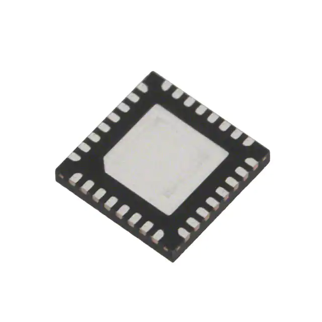
- Part No.:
- SX1255IWLTRT
- Manufacturer:
- Semtech Corporation
- Category:
- RF Transceiver ICs
- Package:
- 32-WFQFN Exposed Pad
- Datasheet:
-
 SX1255IWLTRT.pdf
- Description:
- IC RF TXRX 802.15.4 32MLPQ
- Quantity:
- Payment:

- Shipping:

Inventory:2,865
Please send an inquiry. Send us your inquiry, and we will respond immediately.
Product details
Overview
SX1255IWLTRT from Semtech is a highly integrated Zero-IF RF front-end transceiver IC supporting multi-PHY modulation (MR-FSK, MR-O-QPSK, MR-OFDM) across 400–510 MHz licensed and unlicensed bands. It delivers 500 kHz max signal bandwidth in both TX and RX, −110 dBc/Hz phase noise at 10 kHz offset, 4.5 dB typical noise figure, and programmable analog prefiltering (TX DSB: 420–1700 kHz; RX SSB: 500–1500 kHz), enabling smart grid and SDR applications with minimal external components.
For engineers reviewing the SX1255IWLTRT datasheet, pinout, applications, or equivalent options, this page provides verified technical context, validated pin functions, confirmed regulatory compliance (ETSI/FCC/ARIB), real-world power consumption data (25 mA RX, 90 mA TX), and accurate alternative part comparisons for multi-PHY wireless system design.
Technical Context
The SX1255IWLTRT implements a fractional-N PLL-based frequency synthesizer with 30.5 Hz step resolution and sub-50 µs RX/TX hop time to within 10 kHz, supporting rapid channel switching in cognitive radio systems. Its architecture integrates independent TX and RX analog front-ends with programmable gain control (70 dB RX range), digital I/Q interfaces (I2S-compatible mode A/B), and on-chip FIR-DAC filtering (24–64 taps).
TrueRF™ technology enables ETSI/FCC/ARIB-compliant operation without external RF filters or matching networks. The device supports half/full-duplex operation via software-configurable DIO pins and includes bullet-proof LNA with 4.5 dB NF, linear TX amplifier (up to +7 dBm saturated output), and decimated I/Q outputs compliant with industry-standard baseband processor timing.
Key Specifications
| Parameter | Value and Actual Design Meaning |
|---|---|
| Frequency Range | 400–510 MHz programmable; covers global ISM bands without hardware change. |
| Signal Bandwidth | 500 kHz max in both TX and RX; supports MR-FSK, MR-O-QPSK, and MR-OFDM PHY layers. |
| Noise Figure | 4.5 dB typical (max LNA gain); ensures high sensitivity in low-SNR smart metering environments. |
| Phase Noise | −110 dBc/Hz @ 10 kHz offset; meets spectral mask requirements for narrowband licensed operation. |
| Power Consumption | 25 mA RX typical, 90 mA TX @ −5 dBm; enables battery-powered long-life deployments. |
| Analog Filter BW | TX DSB: 420–1700 kHz; RX SSB: 500–1500 kHz; digitally programmable in fine steps for PHY adaptation. |
| Output Power | +7 dBm saturated; sufficient for 1 km+ range in sub-GHz mesh networks with external PA optional. |
| Regulatory Compliance | FCC Part 15, ETSI EN 300 220, ARIB STD-T67 certified; no external filter required for conformance. |
Pinout & Package
Package: MLPQ-W 5 × 5 mm, 32-lead, exposed pad (RoHS/WEEE compliant). Pin mapping validated per Semtech DS Rev. 3.0, Table 1.
| Pin/Terminal | Circuit Role | Design Meaning |
|---|---|---|
| GND (Pads 0, 4, 7, 26, 28, 31) | Ground reference | Multiple dedicated GND pins and exposed thermal pad ensure low-impedance return paths for analog/digital/RF sections. |
| RFIN (Pin 27) | Receiver input | Differential RF input to LNA; requires external balun for single-ended antenna interface. |
| RFOP / RFON (Pins 29–30) | Transmitter output | Differential TX output; connects directly to balun or PA input without external matching network. |
| I_IN / Q_IN (Pins 12–13) | Digital baseband input | 1-bit serial or I2S-compatible interface for TX I/Q data; supports mode A (master/slave) and mode B timing. |
| I_OUT / Q_OUT (Pins 14–15) | Digital baseband output | Decimated I/Q samples delivered in I2S format; synchronized to CLK_OUT for deterministic latency. |
| NSS / SCK / MOSI / MISO (Pins 20–19–17–18) | SPI control interface | 4-wire SPI for register configuration; operates up to 10 MHz; supports full-duplex status readback. |
| XTA / XTB (Pins 6–8) | Clock source | 32–36.864 MHz crystal or external clock input; enables precise frequency synthesis and low-jitter operation. |
| DIO0–DIO3 (Pins 21–24) | Configurable GPIO | Software-defined digital I/O for interrupt signaling, mode control, or status indication in embedded host systems. |
Key Features
| Feature | Design Value |
|---|---|
| Multi-PHY Modulation Support | Native hardware support for MR-FSK, MR-O-QPSK, and MR-OFDM - eliminates need for FPGA-based waveform generation. |
| Programmable Analog Prefilters | TX DSB and RX SSB bandwidths digitally adjustable in 31 steps - enables dynamic PHY adaptation without PCB changes. |
| TrueRF™ Integration | Meets FCC/ETSI/ARIB spectral masks with zero external RF filters - reduces BOM count and layout complexity. |
| Low-Power Wake-up | 50 µs RX synthesizer wake-up time and 300 µs crystal start-up - enables ultra-low-duty-cycle listening in battery nodes. |
| Flexible Digital Interface | I2S-compatible I/Q interface plus standard SPI - simplifies integration with ARM Cortex-M, DSP, or FPGA baseband processors. |
| Bullet-Proof LNA | 4.5 dB NF with 70 dB gain range and robust 0 dBm input tolerance - maintains performance under strong interferer conditions. |
Applications
| Smart Grid AMI | Industrial SDR Gateway |
|---|---|
|
Use Scenario: Two-way communication between utility meters and concentrators in licensed 450 MHz band. IC Role / Device Role / Timing Role: RF front-end transceiver handling MR-O-QPSK PHY layer with adaptive channel hopping. Use Value: 500 kHz bandwidth and 4.5 dB NF enable reliable reception at −125 dBm sensitivity over 2 km range in noisy substations. |
Use Scenario: Field-deployable spectrum monitoring node using software-defined demodulation of legacy ISM protocols. IC Role / Device Role / Timing Role: Zero-IF analog front-end feeding I/Q samples to FPGA-based demodulator with real-time reconfiguration. Use Value: Programmable TX/RX analog filters and 30.5 Hz frequency step allow precise capture of narrowband signals across 400–510 MHz. |
| Sub-GHz IoT Sensor Hub | Wireless Building Automation |
|
Use Scenario: Battery-powered environmental sensor cluster reporting temperature/humidity via star topology to gateway. IC Role / Device Role / Timing Role: Low-power transceiver operating in MR-FSK mode with duty-cycled RX and fast wake-up. Use Value: 25 mA RX current and 50 µs synthesizer lock time reduce average power to <10 µA in listen-before-talk mode. |
Use Scenario: HVAC controller communicating with thermostats, actuators, and occupancy sensors in commercial buildings. IC Role / Device Role / Timing Role: Full-duplex capable transceiver managing bidirectional command/response traffic with low-latency ACK. Use Value: Half/full-duplex flexibility and DIO0–DIO3 GPIOs enable hardware handshake and priority interrupt signaling without MCU overhead. |
Equivalent & Alternatives
The following parts are listed as comparable options for similar RF front-end transceiver applications.
| Alternative Part | Technical Difference | Application Difference | Selection Advice |
|---|---|---|---|
| SX1276IMLTRT | LoRa®-optimized; narrower max RX BW (500 kHz vs 1500 kHz); higher RX sensitivity (−148 dBm vs −125 dBm) but fixed PHY. | Best for LoRaWAN end-nodes; lacks MR-FSK/MR-OFDM support and programmable analog filtering. | Select SX1255IWLTRT when multi-PHY flexibility and wideband SDR capability are required over pure LoRa range. |
| AD9361BBCZ | Higher integration (dual-band, 2×2 MIMO); wider bandwidth (56 MHz); requires external LO and complex power management. | Targeted at high-throughput SDR base stations; not optimized for sub-GHz licensed band or ultra-low-power sensor nodes. | Choose SX1255IWLTRT for cost-sensitive, single-band, battery-operated smart grid endpoints where 500 kHz BW suffices. |
Compared with SX1276IMLTRT and AD9361BBCZ, the SX1255IWLTRT uniquely balances multi-PHY adaptability, regulatory-ready RF integration, and sub-30 mA receive current - making it optimal for certified, field-deployable sub-GHz wireless infrastructure requiring firmware-upgradable PHYs.
Availability
SX1255IWLTRT is available at Aetrix Electronics and suitable for smart grid AMI deployments, industrial SDR gateways, sub-GHz IoT sensor hubs, and wireless building automation systems requiring stable component supply, long-term lifecycle assurance, and traceable sourcing.
Supply support for SX1255IWLTRT includes scheduled delivery planning, volume procurement assistance, BOM continuity management, traceable sourcing, and lifecycle availability coordination for OEM customers, industrial embedded developers, connected-device designers, and electronics production programs.
Manufacturer
Semtech Corporation is a U.S.-based fabless semiconductor company specializing in high-performance analog and RF solutions for enterprise, industrial, and communications markets.
The SX1255IWLTRT belongs to Semtech's Wireless & Sensing product line, designed specifically for multi-PHY, software-defined sub-GHz wireless systems requiring regulatory compliance, low power, and flexible modulation support.
FAQ
What modulation schemes does the SX1255IWLTRT natively support?
The SX1255IWLTRT natively supports MR-FSK, MR-O-QPSK, and MR-OFDM modulation schemes as defined in IEEE 802.15.4g SUN standard. Its fully flexible I/Q modulator/demodulator allows real-time waveform adaptation without external FPGA logic. All three schemes operate within the 400–510 MHz band and leverage the device's programmable analog prefiltering and TrueRF™ architecture. This capability is explicitly documented in the General Description and Applications sections of the SX1255IWLTRT datasheet Rev. 3.0.
Does the SX1255IWLTRT require external RF filters to meet FCC or ETSI emissions limits?
No, the SX1255IWLTRT does not require external RF filters to meet FCC Part 15, ETSI EN 300 220, or ARIB STD-T67 emissions limits. Its TrueRF™ technology integrates calibrated analog prefiltering, precise DAC/ADC timing, and phase noise suppression to satisfy spectral mask requirements out-of-the-box. The datasheet confirms compliance is achieved with only passive decoupling and matching components - no external bandpass or harmonic filters are needed for certification.
What is the maximum differential RF output power of the SX1255IWLTRT?
The SX1255IWLTRT delivers up to +7 dBm saturated differential RF output power (TXPmax), measured into a 100 Ω load. This value is specified in Table 6 of the SX1255IWLTRT datasheet Rev. 3.0 under "TX Maximum Output Power". For most smart grid and IoT applications, the device is typically operated at −5 dBm to optimize linearity and current consumption, but the +7 dBm headroom supports connection to external power amplifiers when extended range is required.
How many bits per sample does the SX1255IWLTRT use for its I/Q digital interface?
The SX1255IWLTRT uses 1-bit serial data for its primary I/Q interface in Mode A (as master or slave), compatible with standard I2S timing. In Mode B, it supports configurable bit depths including 16-bit, 20-bit, and 24-bit samples depending on sampling rate and mode selection (B1/B2), as detailed in Tables 13–18 of the SX1255IWLTRT datasheet. The 1-bit interface minimizes MCU interface complexity, while Mode B offers higher fidelity for demanding SDR applications.
Is the SX1255IWLTRT pin-compatible with other Semtech transceivers like the SX1276?
No, the SX1255IWLTRT is not pin-compatible with the SX1276IMLTRT or other Semtech transceivers. It uses a unique 32-pin MLPQ-W package with distinct pin assignments - for example, RFIN is on Pin 27, RFOP/RFON on Pins 29–30, and dual I/Q data lines on Pins 12–15. The SX1276 uses a 32-pin QFN but with different pin functions and power domain routing. Board-level replacement requires full schematic and layout revision; no drop-in substitution is possible.
SX1255IWLTRT Specifications
- Product attributes
- Attribute value
- Manufacturer:
- Semtech Corporation
- Series:
- -
- Package/Case:
- 32-WFQFN Exposed Pad
- Packaging:
- Tape & Reel (TR)
- Product Status:
- Active
- Programmable:
- Not Verified
- Type:
- TxRx Only
- RF Family/Standard:
- 802.15.4
- Protocol:
- -
- Modulation:
- FHSS, FSK, OFDM, O-QPSK
- Frequency:
- 400MHz ~ 510MHz
- Data Rate (Max):
- -
- Power - Output:
- 7dbm
- Sensitivity:
- -
- Memory Size:
- -
- Serial Interfaces:
- I2S, SPI
- GPIO:
- 4
- Voltage - Supply:
- 2.7V ~ 3.6V
- Current - Receiving:
- 18mA
- Current - Transmitting:
- 60mA
- Operating Temperature:
- -40°C ~ 85°C
- Grade:
- -
- Qualification:
- -
- Supplier Device Package:
- 32-MLPQ (5x5)
SX1255IWLTRT FAQ
1.How can I place an order for SX1255IWLTRT through Aetrix?
Please submit a Request for Quotation (RFQ) for SX1255IWLTRT on Aetrix. Our sales agent will provide a competitive quotation and guide you through the order confirmation once you accept the terms.
2.Are the price and stock information for SX1255IWLTRT reliable?
The price and inventory of SX1255IWLTRT are updated periodically and may fluctuate due to market conditions. Stock and pricing data are typically refreshed every 24 hours. Quotation validity for SX1255IWLTRT is usually 5 days.
3.What payment methods are accepted for SX1255IWLTRT?
We accept Wire Transfer, PayPal, Credit Card, Western Union, MoneyGram, and Escrow for SX1255IWLTRT transactions.
Note: Certain payment methods may incur a processing fee.
4.How is shipping managed for SX1255IWLTRT?
SX1255IWLTRT orders can be shipped via leading logistics carriers, including DHL, UPS, FedEx, TNT, or Registered Mail.
Once your SX1255IWLTRT order is processed, you will receive an email with the shipment details and tracking number.
Note: Tracking information may take up to 24 hours to appear. Express delivery typically takes 3–5 business days.
5.How can I obtain technical support or documentation for SX1255IWLTRT?
For technical support, including SX1255IWLTRT datasheets, pinout diagrams, or application guidance, please contact our engineering support team. They can provide detailed documentation and assistance for your SX1255IWLTRT requirements.
6.How does Aetrix verify that SX1255IWLTRT is sourced from the original manufacturer or authorized distributors?
All SX1255IWLTRT products on Aetrix are procured from qualified distributors and authorized channels. Our dedicated quality assurance team conducts strict verification, including traceability checks and, if necessary, third-party testing. This ensures that SX1255IWLTRT meets industry standards.
7.What is the process for return or replacement of SX1255IWLTRT?
All SX1255IWLTRT units undergo pre-shipment inspection (PSI). If there is an issue with SX1255IWLTRT, returns or replacements are accepted under the following conditions:
1.Quantity discrepancies, incorrect items, or visible external defects (such as breakage or corrosion), acknowledged by Aetrix.
2.The issue is reported within 90 days of delivery.
3.The SX1255IWLTRT part is unused and in its original packaging.
Return procedure for SX1255IWLTRT:
1.Submit a request within 90 days.
2.Obtain a Return Material Authorization (RMA) from Aetrix.
SX1255IWLTRT Tags

-
ESP32-D0WD-V3
Espressif Systems

-
ESP8266EX
Espressif Systems

-
ESP32-S3
Espressif Systems

-
NRF24L01P-R7
Nordic Semiconductor ASA
-
NRF24L01P-R
Nordic Semiconductor ASA

-
ESP32-U4WDH
Espressif Systems

-
DA14531-00000OG2
Renesas
-
ESP32-C6FH4
Espressif Systems

-
DA14531-00000FX2
Renesas
-
NRF24L01P-T
Nordic Semiconductor ASA

-
NRF52810-QCAA-R
Nordic Semiconductor ASA
-
ESP32-S3FN8
Espressif Systems
Tech Hub

A practical engineering and sourcing framework covering lifecycle verification, lifetime-buy calculations, replacement qualification, supplier checks and counterfeit-risk controls.

TTL and CMOS logic families differ in thresholds, loading, output drive, power and timing. This engineering guide compares 74HC and 74HCT, calculates noise margins and checks 3.3 V/5 V compatibility.

A practical engineering guide to 3.3V and 5V logic compatibility, input thresholds, resistor dividers, translator ICs, MOSFET level shifting, I2C pull-ups, timing limits and power-sequencing risks.

The 74HC595 uses push-pull logic outputs, while the TPIC6B595 uses 50 V open-drain DMOS sinks for higher-power loads. This guide compares timing, current limits, 3.3 V interfacing, load wiring, thermal…

The 74HC595 converts serial data into eight stable parallel outputs. This guide covers pin functions, shift and storage timing, OE and MR behavior, drive-current limits, cascading, voltage compatibilit…

A technical comparison of level-sensitive latches and edge-triggered flip-flops, covering timing windows, setup and hold limits, master–slave operation, time borrowing, race-through, HDL inference and…

A D latch stores one bit while Enable controls when data can pass. This reference covers gate-level operation, truth tables, transparency, setup and hold timing, LE versus OE, common ICs and practical …

An SR latch stores one bit through cross-coupled feedback. This engineering reference covers NOR and NAND implementations, truth tables, forbidden-state recovery, gated operation, switch debouncing, fa…

Latch circuits retain one bit through feedback. This technical reference covers SR and D latches, truth tables, transparency, timing limits, latch-versus-flip-flop behavior, applications and common log…

An engineering guide to LED driver operation, constant-current and constant-voltage outputs, linear and switching topologies, dimming, IC selection, calculations, replacement compatibility, and fault c…


