
 My Inquiry
 My Account


Semtech Corporation SX1441I077TRLF
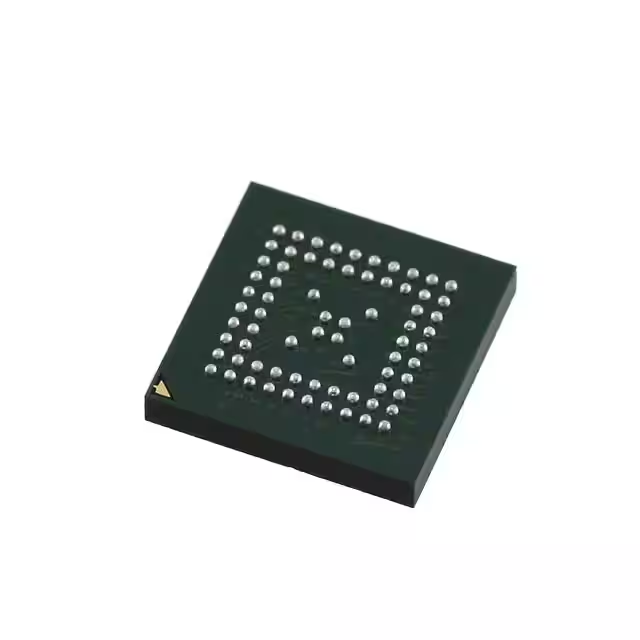
- Part No.:
- SX1441I077TRLF
- Manufacturer:
- Semtech Corporation
- Category:
- RF Transceiver ICs
- Package:
- 72-LFBGA
- Datasheet:
-
 SX1441I077TRLF.pdf
- Description:
- IC RF TXRX+MCU BLE 72LFBGA
- Quantity:
- Payment:

- Shipping:

Inventory:2,326
Please send an inquiry. Send us your inquiry, and we will respond immediately.
Product details
Overview
SX1441I077TRLF from Semtech is a Bluetooth® 1.2 System-on-Chip integrating an 8-bit CoolRISC CPU, on-chip 16-bit linear audio CODEC with DMA, high-speed UART (up to 921 kbit/s), SPI interface, and power management unit. It supports simultaneous SCO + three ACL links, AFH, Fast Connect, and eSCO - designed for ultra-low-power wireless headsets consuming <23 mW at 1.8 V.
For engineers reviewing the SX1441I077TRLF datasheet, pinout, applications, or equivalent options, key selection considerations include Bluetooth 1.2 stack compliance up to HCI, integrated battery-level detection, dual-regulator supply architecture (VREGA/VREGD), and compatibility with Semtech XE1413 radio for complete headset BOM minimization.
Technical Context
The SX1441I077TRLF implements an embedded-host architecture: the ROM-based Bluetooth Sequencer handles Link Controller/Manager and HCI layers independently of the application CPU, ensuring real-time protocol execution without software interference. Its clock system includes dual sources - 13 MHz crystal (SYS_CLOCK_IN) and 32 kHz slow clock (SLW_CLK_IN) - with internal RC oscillator backup.
Power management integrates analog/digital regulators (VREGA, VREGD), battery end-of-life (EOL) monitoring via VDDBAT input, and five operating modes (Active, Idle, Sleep, Deep Sleep, Off). The audio subsystem features differential microphone inputs (VMIC_P/VMIC_N), stereo-capable CODEC, and integrated Class-D PA outputs (PA_OUTP/PA_OUTN) supporting direct speaker drive.
Key Specifications
| Parameter | Value and Actual Design Meaning |
|---|---|
| Bluetooth Standard | Compliant with Bluetooth v1.2 specification including AFH, Fast Connect, and eSCO - enables robust voice links in noisy 2.4 GHz environments. |
| CPU Core | CoolRISC 816 8-bit RISC processor with single-cycle instruction execution - optimized for low-power application control and upper-layer stack processing. |
| Audio Interface | On-chip 16-bit linear PCM CODEC with DMA, VMIC_P/VMIC_N differential input, and PA_OUTP/PA_OUTN Class-D outputs - eliminates external audio codec and amplifier components. |
| UART Speed | High-speed UART supporting up to 921 kbit/s with hardware flow control (RTS/CTS) - suitable for host MCU communication or HCI transport. |
| Supply Range | 1.8 V to 3.6 V operation with dedicated VDD_M, VDD_PA, VDD_DIG, VDD_ANA rails - enables flexible power domain partitioning and battery voltage scaling. |
| Radio Interface | Dedicated SPI-based radio interface (SPI_DATA_IN/OUT, SPI_CLK_OUT, SPI_EN_BAR, TX_EN, RX_EN) - designed for seamless integration with Semtech XE1413 or CX72303 radios. |
| Package | 72-pin LFBGA (7 mm × 7 mm, 0.5 mm pitch) - compact footprint for space-constrained headset PCBs with thermal pad for power dissipation. |
Pinout & Package
72-pin Low-Profile Fine-Pitch Ball Grid Array (LFBGA) package with exposed thermal pad; dimensions 7 mm × 7 mm, pitch 0.5 mm. Pin mapping conforms to bottom-view layout per Semtech DS Rev 4 (July 2006).
| Pin/Terminal | Circuit Role | Design Meaning |
|---|---|---|
| NRESET | Master reset input | Active-low asynchronous reset signal referenced to VDD_M - initiates full chip initialization sequence. |
| PA[7:0] | Digital input port A | Eight dedicated GPIO inputs (no output capability) with internal pull-up/down - used for button sensing, status monitoring, or wake-up triggers. |
| PB[7:0] | Digital I/O port B | Eight bidirectional GPIO pins supporting UART (TX/RX/RTS/CTS), configurable as general-purpose signals - enables flexible peripheral interfacing. |
| MOSI/MISO/SCK/NSS[4:0] | SPI interface | Five independent slave select lines support daisy-chained or parallel flash memory and radio coexistence - critical for multi-peripheral SoC designs. |
| VMIC_P / VMIC_N | Differential microphone input | Low-noise analog front-end with programmable gain - accepts electret microphone signals directly without external amplification. |
| PA_OUTP / PA_OUTN | Differential speaker output | Class-D power amplifier outputs driving 8 Ω speakers - delivers >100 mW output with integrated feedback loop and EMI suppression. |
| VDDIO_DIG / VDDIO | Digital I/O supply domains | Separate 1.8–3.6 V supplies for digital pads (VDDIO_DIG) and radio interface (VDDIO) - isolates noise-sensitive RF paths from logic switching. |
Key Features
| Feature | Design Value |
|---|---|
| Embedded-Host Architecture | Independent Bluetooth Sequencer (ROM-based protocol stack) and application CPU eliminate software validation burden for Bluetooth qualification. |
| Integrated Power Management | VREGA (analog) and VREGD (digital) regulators with battery EOL detection via VDDBAT input - enables autonomous low-battery shutdown without host intervention. |
| Dual-Clock Domain Support | Simultaneous 13 MHz SYS_CLOCK_IN and 32 kHz SLW_CLK_IN inputs - allows precise timing for Bluetooth packet scheduling and low-power sleep mode retention. |
| Hardware UART Flow Control | Full RTS/CTS handshaking implemented in silicon - prevents data loss during high-throughput HCI communication with host processors. |
| Radio Interface Optimization | Dedicated SPI control lines (SPI_EN_BAR, TX_EN, RX_EN, SYNC_DETECT) synchronized to radio timing - ensures deterministic radio state transitions and minimal latency. |
Applications
| Wireless Headset | Handsfree Car Kit |
|---|---|
|
Use Scenario: Compact mono/stereo earpiece with microphone and speaker, powered by single Li-ion cell. IC Role / Device Role / Timing Role: Primary Bluetooth SoC handling baseband, link layer, HCI, audio CODEC, and power management - serves as central timing and control hub. Use Value: Eliminates need for external MCU, audio codec, and PMIC; enables sub-23 mW active power consumption at 1.8 V. |
Use Scenario: Vehicle-mounted speakerphone with push-to-talk button, LED status indicators, and echo cancellation. IC Role / Device Role / Timing Role: Host processor for handsfree profile (HFP), managing audio routing, call signaling, and GPIO-driven user interface. Use Value: On-chip SCO channel support and eSCO enable wideband voice with low-latency audio path; PB[7:0] GPIOs directly drive LEDs and buttons. |
| VoIP/Bluetooth Gateway | Cable Replacement Module |
|
Use Scenario: USB-to-Bluetooth adapter bridging PC VoIP clients to Bluetooth headsets. IC Role / Device Role / Timing Role: Bluetooth controller with UART-based HCI transport to host PC - provides certified Bluetooth link layer and audio transport. Use Value: Fully compliant Bluetooth 1.2 stack up to HCI reduces host-side driver complexity; UART supports 921 kbit/s for low-latency audio streaming. |
Use Scenario: Embedded module replacing RS-232 or USB cables between industrial sensors and controllers. IC Role / Device Role / Timing Role: Data-centric Bluetooth SoC establishing ACL links for transparent serial data tunneling - operates without audio subsystem activation. Use Value: Supports up to three concurrent ACL connections; NSS[4:0] enables multiplexing of multiple peripherals (e.g., flash, sensor ICs) over shared SPI bus. |
Equivalent & Alternatives
The following parts are listed as comparable options for similar Bluetooth SoC applications.
| Alternative Part | Technical Difference | Application Difference | Selection Advice |
|---|---|---|---|
| CSR BC417143 | ARM7TDMI core, integrated flash, no on-chip CODEC - requires external audio components and separate PMIC. | Targeted at higher-BOM-cost headsets needing larger code space; lacks integrated battery monitoring. | Select when firmware complexity exceeds SX1441I077TRLF's ROM+external flash architecture and external audio path is acceptable. |
| Texas Instruments CC2564C | Bluetooth 4.0 dual-mode (BR/EDR + BLE), 32-bit ARM Cortex-M3, integrated RF balun - supports modern profiles but higher active current (~30 mA). | Designed for BLE+BR/EDR convergence; not pin-compatible and requires different layout, antenna, and power design. | Choose for new designs requiring Bluetooth Smart readiness or multi-role connectivity; not a drop-in replacement. |
Compared with CSR BC417143 and CC2564C, the SX1441I077TRLF offers lowest BOM count for Bluetooth 1.2 voice applications due to integrated CODEC, PA, and dual-regulator PMU - but lacks BLE support and has smaller program memory footprint.
Availability
SX1441I077TRLF is available at Aetrix Electronics and suitable for wireless headset, handsfree car kit, and VoIP gateway applications requiring stable component supply, long-lifecycle support, and qualified Bluetooth 1.2 silicon.
Supply support for SX1441I077TRLF includes scheduled delivery planning, volume procurement assistance, BOM continuity management, traceable sourcing, and lifecycle availability coordination for OEM customers, industrial embedded developers, connected-device designers, and electronics production programs.
Manufacturer
Semtech Corporation is a U.S.-based semiconductor company specializing in high-performance analog and mixed-signal semiconductors for enterprise computing, communications, and industrial markets.
The SX1441I077TRLF belongs to Semtech's EasyBlue™ family of Bluetooth SoCs, engineered specifically for ultra-low-power voice-centric wireless accessories - emphasizing integration, qualification readiness, and minimal external component count.
FAQ
What Bluetooth profiles does the SX1441I077TRLF natively support?
The SX1441I077TRLF implements the Bluetooth 1.2 baseband, Link Controller, Link Manager, and HCI layers in ROM. Profile support (e.g., HSP, HFP, SPP) is determined by the upper-layer stack loaded into external flash memory. The SX1441I077TRLF itself provides certified, qualified lower-layer compliance - enabling third-party or custom profile implementations without requalification.
Does the SX1441I077TRLF require an external crystal oscillator?
Yes, the SX1441I077TRLF requires a 13 MHz fundamental-mode crystal connected to SYS_CLOCK_IN (Pin J9) for primary Bluetooth timing. It also supports a 32 kHz watch crystal on SLW_CLK_IN (Pin K3) for low-power sleep mode timing. An internal RC oscillator serves only as backup - not for Bluetooth packet timing accuracy.
Can the SX1441I077TRLF operate without the integrated audio CODEC enabled?
Yes, the SX1441I077TRLF can be configured to disable the audio CODEC and use only its UART, SPI, GPIO, and Bluetooth baseband functions. This is typical in cable-replacement or data-tunneling applications. The VMIC_P/VMIC_N and PA_OUTP/PA_OUTN pins become no-connect, and associated analog power domains (VDD_ANA, VREGA) may be unpowered.
What is the function of the VDDBAT pin on the SX1441I077TRLF?
The VDDBAT pin (Pin C2) is an analog input used for battery end-of-life (EOL) detection. It connects directly to the battery terminal and feeds an internal comparator that triggers a flag when voltage drops below a programmable threshold - enabling autonomous low-battery shutdown without host MCU involvement. This feature is integral to the SX1441I077TRLF's power management unit.
Is the SX1441I077TRLF pin-compatible with other members of the EasyBlue™ family?
No, the SX1441I077TRLF is not pin-compatible with other EasyBlue™ devices such as SX1212 or SX1442. Its 72-pin LFBGA package, pin assignment (e.g., dedicated PA_OUTP/PA_OUTN, five NSS lines, DBG[7:0] debug interface), and power domain layout are unique to the SX1441I077TRLF. Migration requires PCB redesign and firmware adaptation.
SX1441I077TRLF Specifications
- Product attributes
- Attribute value
- Manufacturer:
- Semtech Corporation
- Series:
- -
- Package/Case:
- 72-LFBGA
- Packaging:
- Tape & Reel (TR)
- Product Status:
- Obsolete
- Programmable:
- Not Verified
- Type:
- TxRx + MCU
- RF Family/Standard:
- Bluetooth
- Protocol:
- Bluetooth v1.2
- Modulation:
- -
- Frequency:
- 2.4GHz
- Data Rate (Max):
- 921kbps
- Power - Output:
- -
- Sensitivity:
- -
- Memory Size:
- 4kB ROM, 40kB RAM
- Serial Interfaces:
- SPI, UART
- GPIO:
- 8
- Voltage - Supply:
- 2V ~ 3.6V
- Current - Receiving:
- -
- Current - Transmitting:
- -
- Operating Temperature:
- -40°C ~ 85°C
- Grade:
- -
- Qualification:
- -
- Supplier Device Package:
- 72-LFBGA (7x7)
SX1441I077TRLF FAQ
1.How can I place an order for SX1441I077TRLF through Aetrix?
Please submit a Request for Quotation (RFQ) for SX1441I077TRLF on Aetrix. Our sales agent will provide a competitive quotation and guide you through the order confirmation once you accept the terms.
2.Are the price and stock information for SX1441I077TRLF reliable?
The price and inventory of SX1441I077TRLF are updated periodically and may fluctuate due to market conditions. Stock and pricing data are typically refreshed every 24 hours. Quotation validity for SX1441I077TRLF is usually 5 days.
3.What payment methods are accepted for SX1441I077TRLF?
We accept Wire Transfer, PayPal, Credit Card, Western Union, MoneyGram, and Escrow for SX1441I077TRLF transactions.
Note: Certain payment methods may incur a processing fee.
4.How is shipping managed for SX1441I077TRLF?
SX1441I077TRLF orders can be shipped via leading logistics carriers, including DHL, UPS, FedEx, TNT, or Registered Mail.
Once your SX1441I077TRLF order is processed, you will receive an email with the shipment details and tracking number.
Note: Tracking information may take up to 24 hours to appear. Express delivery typically takes 3–5 business days.
5.How can I obtain technical support or documentation for SX1441I077TRLF?
For technical support, including SX1441I077TRLF datasheets, pinout diagrams, or application guidance, please contact our engineering support team. They can provide detailed documentation and assistance for your SX1441I077TRLF requirements.
6.How does Aetrix verify that SX1441I077TRLF is sourced from the original manufacturer or authorized distributors?
All SX1441I077TRLF products on Aetrix are procured from qualified distributors and authorized channels. Our dedicated quality assurance team conducts strict verification, including traceability checks and, if necessary, third-party testing. This ensures that SX1441I077TRLF meets industry standards.
7.What is the process for return or replacement of SX1441I077TRLF?
All SX1441I077TRLF units undergo pre-shipment inspection (PSI). If there is an issue with SX1441I077TRLF, returns or replacements are accepted under the following conditions:
1.Quantity discrepancies, incorrect items, or visible external defects (such as breakage or corrosion), acknowledged by Aetrix.
2.The issue is reported within 90 days of delivery.
3.The SX1441I077TRLF part is unused and in its original packaging.
Return procedure for SX1441I077TRLF:
1.Submit a request within 90 days.
2.Obtain a Return Material Authorization (RMA) from Aetrix.
SX1441I077TRLF Tags

-
ESP32-D0WD-V3
Espressif Systems

-
ESP8266EX
Espressif Systems

-
ESP32-S3
Espressif Systems

-
NRF24L01P-R7
Nordic Semiconductor ASA
-
NRF24L01P-R
Nordic Semiconductor ASA

-
ESP32-U4WDH
Espressif Systems

-
DA14531-00000OG2
Renesas
-
ESP32-C6FH4
Espressif Systems

-
DA14531-00000FX2
Renesas
-
NRF24L01P-T
Nordic Semiconductor ASA

-
NRF52810-QCAA-R
Nordic Semiconductor ASA
-
ESP32-S3FN8
Espressif Systems
Tech Hub

A practical engineering and sourcing framework covering lifecycle verification, lifetime-buy calculations, replacement qualification, supplier checks and counterfeit-risk controls.

TTL and CMOS logic families differ in thresholds, loading, output drive, power and timing. This engineering guide compares 74HC and 74HCT, calculates noise margins and checks 3.3 V/5 V compatibility.

A practical engineering guide to 3.3V and 5V logic compatibility, input thresholds, resistor dividers, translator ICs, MOSFET level shifting, I2C pull-ups, timing limits and power-sequencing risks.

The 74HC595 uses push-pull logic outputs, while the TPIC6B595 uses 50 V open-drain DMOS sinks for higher-power loads. This guide compares timing, current limits, 3.3 V interfacing, load wiring, thermal…

The 74HC595 converts serial data into eight stable parallel outputs. This guide covers pin functions, shift and storage timing, OE and MR behavior, drive-current limits, cascading, voltage compatibilit…

A technical comparison of level-sensitive latches and edge-triggered flip-flops, covering timing windows, setup and hold limits, master–slave operation, time borrowing, race-through, HDL inference and…

A D latch stores one bit while Enable controls when data can pass. This reference covers gate-level operation, truth tables, transparency, setup and hold timing, LE versus OE, common ICs and practical …

An SR latch stores one bit through cross-coupled feedback. This engineering reference covers NOR and NAND implementations, truth tables, forbidden-state recovery, gated operation, switch debouncing, fa…

Latch circuits retain one bit through feedback. This technical reference covers SR and D latches, truth tables, transparency, timing limits, latch-versus-flip-flop behavior, applications and common log…

An engineering guide to LED driver operation, constant-current and constant-voltage outputs, linear and switching topologies, dimming, IC selection, calculations, replacement compatibility, and fault c…


