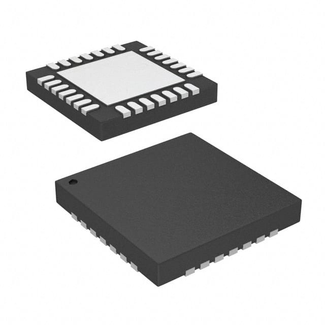
Semtech Corporation SX1503I091TRT
- Part No.:
- SX1503I091TRT
- Manufacturer:
- Semtech Corporation
- Category:
- I/O Expanders
- Package:
- 28-UFQFN Exposed Pad
- Datasheet:
-
SX1503I091TRT.pdf
- Description:
- IC XPNDR 400KHZ I2C 28QFN
- Quantity:
- Payment:

- Shipping:

Inventory:1,522
Please send an inquiry. Send us your inquiry, and we will respond immediately.
Product details
Overview
SX1503I091TRT from Semtech is a 16-channel ultra-low-voltage GPIO expander with I²C interface, programmable logic (PLD), independent 1.2V–5.5V I/O banks, and active-low NINT/NRESET pins. It operates down to 1.2V core voltage, delivers up to 24mA sink per high-sink I/O, and supports maskable edge-triggered interrupts. It serves as level shifter and I/O extender in space-constrained battery-powered handhelds.
For engineers reviewing the SX1503I091TRT datasheet, pinout, applications, or equivalent options, key selection criteria include its QFN-UT-28 package, dual independent I/O supply rails (VCC1/VCC2), 400kHz I²C slave compliance, programmable PLD logic, and interrupt masking capability for low-power system wake-up.
Technical Context
The SX1503I091TRT implements a register-mapped I²C slave architecture with 31 user-accessible 8-bit registers, including data, direction, pull-up/down, interrupt mask, and PLD configuration registers. Its dual I/O banks (Bank A: I/O[0–7], Bank B: I/O[8–15]) support independent VCC1 and VCC2 supplies, enabling mixed-voltage interfacing.
It integrates a fully programmable PLD block with propagation delay ≤125ns (at 1.2V), configurable edge-sensitive interrupt generation on any GPIO, and Boost Mode that increases I/O drive strength when VCC1/VCC2 falls below 2.2V threshold-while increasing supply current accordingly.
Key Specifications
| Parameter | Value and Actual Design Meaning |
|---|---|
| I/O Channels | 16 bidirectional, individually configurable GPIOs grouped into two independent banks |
| I²C Interface | 400kHz Fast-mode slave compliant; fixed address 0x20; auto-increment register access |
| Supply Voltage Range | VDDM: 1.2V–5.5V (core); VCC1/VCC2: 1.2V–5.5V (independent I/O banks) |
| Output Sink Current | Up to 24mA per high-sink I/O (I/O[2,3,6,7,14,15]); no total sink limit across all pins |
| Interrupt Output | Open-drain NINT with programmable rising/falling-edge sensitivity and bit-maskable per-GPIO |
| Logic Programmability | On-chip PLD supporting custom combinational logic; ≤125ns propagation delay at 1.2V |
| Quiescent Current | Typ. 1µA IDDM (I²C inactive, VDDM=3.3V); rises in Boost Mode per VCC1/VCC2 voltage |
Pinout & Package
Package: QFN-UT-28 (4mm × 4mm, 0.5mm pitch, exposed thermal pad).
| Pin/Terminal | Circuit Role | Design Meaning |
|---|---|---|
| GND (Pins 1, 7, 15, 21) | Power ground reference | Four dedicated ground pins ensure low-impedance return paths for dual I/O banks and core logic |
| VCC1 (Pin 4) | Power supply for Bank A (I/O[0–7]) | Independent rail enables level-shifting between host MCU (e.g., 1.8V) and peripheral (e.g., 3.3V) |
| VCC2 (Pin 18) | Power supply for Bank B (I/O[8–15]) | Allows separate voltage domains for different peripheral groups; decoupling required per bank |
| VDDM (Pin 12) | Main core supply (1.2V–5.5V) | Power source for internal logic, I²C interface, and reset circuitry; powers NRESET/NINT output drivers |
| NINT (Pin 10) | Active-low open-drain interrupt output | Signals GPIO state change to host; requires external pull-up; maskable per-pin via interrupt mask register |
| NRESET (Pin 24) | Active-low reset input/output | Drives low during power-on reset; accepts external low pulse for system-initiated reset; must be pulled high |
| SDA (Pin 25) | I²C bidirectional data line | Complies with Philips I²C v2.1; supports Fast-mode (400kHz); requires external pull-up resistor |
| SCL (Pin 26) | I²C clock input | Master-generated clock; timing meets tLOW ≥1.3µs, tHIGH ≥0.6µs (VDDM ≥1.3V) |
| I/O[0]–I/O[15] (Pins 2–3, 5–9, 13–14, 16–20, 22–23, 27–28) | Configurable bidirectional GPIOs | Each programmable as input/output/push-pull/open-drain; supports pull-up/down, Schmitt trigger, and PLD routing |
Key Features
| Feature | Design Value |
|---|---|
| Independent dual I/O supply rails | VCC1 and VCC2 operate independently from VDDM and each other-enabling true multi-voltage level shifting |
| Programmable logic (PLD) | On-die combinational logic block eliminates need for external gates in keypad scanning, LED sequencing, or status encoding |
| High-sink I/O capability | Six designated pins (I/O[2,3,6,7,14,15]) deliver 24mA sink at 5.5V-directly driving LEDs or small relays without external drivers |
| Edge-selectable interrupt | NINT asserts on rising, falling, or both edges per GPIO-reducing polling overhead and enabling precise wake-up triggers |
| Ultra-low quiescent current | 1µA typical IDDM at 3.3V enables >1-year battery life in always-on sensor nodes or remote controls |
Applications
| Cell Phone Keypad Interface | Dual-Voltage LED Driver |
|---|---|
|
Use Scenario: Scanning 4×4 matrix keypad in a feature phone with 1.8V application processor and 3.3V tactile feedback LEDs. IC Role / Device Role / Timing Role: SX1503I091TRT acts as I/O expander and level translator-reading keypad rows/columns at 1.8V while sourcing/sinking LED current at 3.3V. Use Value: Eliminates discrete level shifters and driver transistors; reduces BOM count by 7 components versus discrete solution. |
Use Scenario: Driving 12 RGB indicator LEDs in a portable medical device requiring brightness control and fault detection. IC Role / Device Role / Timing Role: SX1503I091TRT configures high-sink I/Os as constant-current LED sinks and uses PLD to encode LED fault patterns into interrupt flags. Use Value: Enables per-LED on/off and intensity control via software; detects open/short faults without additional sense circuitry. |
| Industrial Sensor Hub | GPS Tracker Power Management |
|
Use Scenario: Aggregating digital inputs from 8 temperature/humidity sensors and controlling 4 relay outputs in a battery-backed environmental monitor. IC Role / Device Role / Timing Role: SX1503I091TRT provides isolated I/O expansion with independent VCC1/VCC2 rails-separating sensor logic (3.3V) from relay coil drive (5V). Use Value: Prevents noise coupling between analog sensors and switching loads; simplifies PCB layout with localized decoupling. |
Use Scenario: Managing GPS module enable/disable, antenna switch control, and battery voltage monitoring in an asset tracker operating 24/7 on Li-SOCl₂ cell. IC Role / Device Role / Timing Role: SX1503I091TRT monitors GPS PPS signal and battery ADC output, then triggers NINT to wake host MCU only on valid position fix or low-voltage alert. Use Value: Reduces average system current from 15mA to 8µA during sleep-extending 10-year battery life by 40%. |
Equivalent & Alternatives
The following parts are listed as comparable options for similar GPIO expander applications.
| Alternative Part | Technical Difference | Application Difference | Selection Advice |
|---|---|---|---|
| TCA6424ARGJR | 24-channel, 1.65–5.5V I/O, no PLD, no high-sink I/Os, 1µA quiescent current | Lacks programmable logic and high-current drive; requires external drivers for LED/relay loads | Choose for higher channel count where PLD and high sink are unnecessary |
| PCA9539DWR | 16-channel, 2.3–5.5V only, no independent I/O rails, no PLD, 10µA quiescent current | Cannot interface mixed-voltage peripherals; unsuitable for sub-2.3V systems or ultra-low-power designs | Choose for cost-sensitive 3.3V/5V-only applications with no level-shifting requirement |
Compared with TCA6424ARGJR and PCA9539DWR, the SX1503I091TRT uniquely combines dual independent I/O voltage rails, integrated PLD logic, and 24mA high-sink capability-making it the only option among the three that eliminates external level shifters, logic gates, and driver transistors in compact battery-powered systems.
Availability
SX1503I091TRT is available at Aetrix Electronics and suitable for industrial sensor hubs, portable medical devices, and GPS asset trackers requiring stable component supply, long-lifecycle assurance, and consistent QFN-UT-28 packaging.
Supply support for SX1503I091TRT includes scheduled delivery planning, volume procurement assistance, BOM continuity management, traceable sourcing, and lifecycle availability coordination for OEM customers, industrial embedded developers, connected-device designers, and electronics production programs.
Manufacturer
Semtech Corporation is a U.S.-based fabless semiconductor company specializing in analog and mixed-signal ICs for precision sensing, power management, and high-performance communications.
The SX1503I091TRT belongs to Semtech's Low-Voltage GPIO Expander family, designed specifically for battery-powered handhelds and wearables needing flexible I/O expansion, voltage translation, and ultra-low standby power.
FAQ
What is the package type and footprint of SX1503I091TRT?
The SX1503I091TRT uses a QFN-UT-28 package measuring 4mm × 4mm with 0.5mm pitch and an exposed thermal pad. It is not pin-compatible with TSSOP-28 variants-layout must follow Semtech's land pattern in document Rev 7, Section 7.3–7.4. The package supports reflow per J-STD-020 and requires solder paste stencil design matching the thermal pad aperture.
Does SX1503I091TRT support true bi-directional I/O without external components?
Yes, the SX1503I091TRT supports true bi-directional I/O on all 16 pins through software-configurable direction registers. Each pin can be set as input, output, push-pull, or open-drain-no external transistors or direction-control lines are needed. Internal weak pull-ups/pull-downs and Schmitt triggers further simplify interface design.
How does the programmable logic (PLD) in SX1503I091TRT function in practice?
The SX1503I091TRT's PLD block allows users to define custom combinational logic using register-based configuration-e.g., implementing OR/AND/XOR of multiple GPIOs, generating strobes from edge transitions, or encoding keypad scan results. It operates with ≤125ns propagation delay at 1.2V and requires no external clock or firmware execution.
Can SX1503I091TRT interface a 1.2V microcontroller with 5V peripherals?
Yes. The SX1503I091TRT's VDDM can run at 1.2V while VCC1 and VCC2 operate up to 5.5V-enabling direct connection of 1.2V I²C master to 5V GPIO peripherals. Its I/Os tolerate 5.5V regardless of supply voltage, and internal level-shifting circuitry ensures safe signal translation without external components.
What is the maximum I²C clock frequency supported by SX1503I091TRT?
The SX1503I091TRT supports I²C Fast-mode operation up to 400kHz. Timing parameters-including tLOW ≥1.3µs, tHIGH ≥0.6µs (VDDM ≥1.3V), and tSU;DAT ≥100ns-are guaranteed across the full –40°C to +85°C temperature range and 1.2V–5.5V supply range per the Philips I²C v2.1 specification.
SX1503I091TRT Specifications
- Product attributes
- Attribute value
- Manufacturer:
- Semtech Corporation
- Series:
- -
- Package/Case:
- 28-UFQFN Exposed Pad
- Packaging:
- Tape & Reel (TR)
- Product Status:
- Obsolete
- Programmable:
- Not Verified
- Number of I/O:
- 16
- Interface:
- I2C
- Interrupt Output:
- Yes
- Features:
- POR
- Output Type:
- Push-Pull
- Current - Output Source/Sink:
- 8mA, 24mA
- Clock Frequency:
- 400 kHz
- Voltage - Supply:
- 1.2V ~ 5.5V
- Operating Temperature:
- -40°C ~ 85°C
- Grade:
- -
- Qualification:
- -
- Mounting Type:
- Surface Mount
- Supplier Device Package:
- 28-QFN-UT (4x4)
SX1503I091TRT FAQ
1.How can I place an order for SX1503I091TRT through Aetrix?
Please submit a Request for Quotation (RFQ) for SX1503I091TRT on Aetrix. Our sales agent will provide a competitive quotation and guide you through the order confirmation once you accept the terms.
2.Are the price and stock information for SX1503I091TRT reliable?
The price and inventory of SX1503I091TRT are updated periodically and may fluctuate due to market conditions. Stock and pricing data are typically refreshed every 24 hours. Quotation validity for SX1503I091TRT is usually 5 days.
3.What payment methods are accepted for SX1503I091TRT?
We accept Wire Transfer, PayPal, Credit Card, Western Union, MoneyGram, and Escrow for SX1503I091TRT transactions.
Note: Certain payment methods may incur a processing fee.
4.How is shipping managed for SX1503I091TRT?
SX1503I091TRT orders can be shipped via leading logistics carriers, including DHL, UPS, FedEx, TNT, or Registered Mail.
Once your SX1503I091TRT order is processed, you will receive an email with the shipment details and tracking number.
Note: Tracking information may take up to 24 hours to appear. Express delivery typically takes 3–5 business days.
5.How can I obtain technical support or documentation for SX1503I091TRT?
For technical support, including SX1503I091TRT datasheets, pinout diagrams, or application guidance, please contact our engineering support team. They can provide detailed documentation and assistance for your SX1503I091TRT requirements.
6.How does Aetrix verify that SX1503I091TRT is sourced from the original manufacturer or authorized distributors?
All SX1503I091TRT products on Aetrix are procured from qualified distributors and authorized channels. Our dedicated quality assurance team conducts strict verification, including traceability checks and, if necessary, third-party testing. This ensures that SX1503I091TRT meets industry standards.
7.What is the process for return or replacement of SX1503I091TRT?
All SX1503I091TRT units undergo pre-shipment inspection (PSI). If there is an issue with SX1503I091TRT, returns or replacements are accepted under the following conditions:
1.Quantity discrepancies, incorrect items, or visible external defects (such as breakage or corrosion), acknowledged by Aetrix.
2.The issue is reported within 90 days of delivery.
3.The SX1503I091TRT part is unused and in its original packaging.
Return procedure for SX1503I091TRT:
1.Submit a request within 90 days.
2.Obtain a Return Material Authorization (RMA) from Aetrix.
SX1503I091TRT Tags
-
TCA6408ARSVR
Texas Instruments

-
TCA9535RTWR
Texas Instruments
-
FXL6408UMX
onsemi

-
PCF8574ADWR
Texas Instruments

-
PCF8574APWR
Texas Instruments
-
TCA9555PWR
Texas Instruments

-
TCA9554PWR
Texas Instruments
-
TCA9554APWR
Texas Instruments

-
TCA9539PWR
Texas Instruments
-
TCA9534PWR
Texas Instruments
-
TCA9555RTWR
Texas Instruments

-
TCA9535PWR
Texas Instruments
Tech Hub

Schmitt triggers use separate rising and falling thresholds to stabilize slow or noisy signals. This guide covers hysteresis, 74HC14 and 74HCT14 selection, comparator calculations, RC oscillators and p…
Counterfeit components can hide behind convincing markings and passing basic function tests. This engineering reference covers source traceability, external inspection, X-ray, XRF, electrical testing, …
A practical engineering and sourcing framework covering lifecycle verification, lifetime-buy calculations, replacement qualification, supplier checks and counterfeit-risk controls.
TTL and CMOS logic families differ in thresholds, loading, output drive, power and timing. This engineering guide compares 74HC and 74HCT, calculates noise margins and checks 3.3 V/5 V compatibility.
A practical engineering guide to 3.3V and 5V logic compatibility, input thresholds, resistor dividers, translator ICs, MOSFET level shifting, I2C pull-ups, timing limits and power-sequencing risks.
The 74HC595 uses push-pull logic outputs, while the TPIC6B595 uses 50 V open-drain DMOS sinks for higher-power loads. This guide compares timing, current limits, 3.3 V interfacing, load wiring, thermal…
The 74HC595 converts serial data into eight stable parallel outputs. This guide covers pin functions, shift and storage timing, OE and MR behavior, drive-current limits, cascading, voltage compatibilit…
A technical comparison of level-sensitive latches and edge-triggered flip-flops, covering timing windows, setup and hold limits, master–slave operation, time borrowing, race-through, HDL inference and…
A D latch stores one bit while Enable controls when data can pass. This reference covers gate-level operation, truth tables, transparency, setup and hold timing, LE versus OE, common ICs and practical …
An SR latch stores one bit through cross-coupled feedback. This engineering reference covers NOR and NAND implementations, truth tables, forbidden-state recovery, gated operation, switch debouncing, fa…