
 My Inquiry
 My Account


Microchip Technology SY10E445JZ-TR
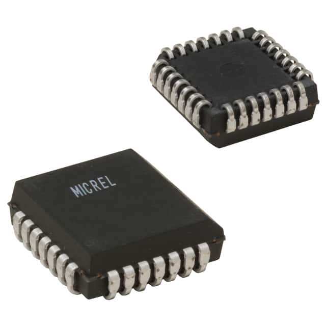
- Part No.:
- SY10E445JZ-TR
- Manufacturer:
- Microchip Technology
- Category:
- Specialized
- Package:
- 28-LCC (J-Lead)
- Datasheet:
-
 SY10E445JZ-TR.pdf
- Description:
- IC INTERFACE SPECIALIZED 28PLCC
- Quantity:
- Payment:

- Shipping:

Inventory:4,288
Please send an inquiry. Send us your inquiry, and we will respond immediately.
Product details
Overview
SY10E445JZ-TR from Micrel is a 4-bit ECL serial-to-parallel converter with differential clock and data inputs, supporting up to 2.5 Gb/s NRZ data rates, on-chip ÷4 and ÷8 clock outputs, and MODE-selectable 4-bit/8-bit operation in a 28-pin PLCC package. It serves as a high-speed demultiplexer in optical interconnect and backplane receiver systems.
For engineers reviewing the SY10E445JZ-TR datasheet, SY10E445JZ-TR pinout, SY10E445JZ-TR application, or SY10E445JZ-TR equivalent, key selection criteria include its 2.5 Gb/s NRZ capability, differential CLK/SIN/SOUT signaling, VBB reference for single-ended use, asynchronous SYNC-controlled bit alignment, and compatibility with MC10E/100E445 timing and logic families.
Technical Context
The SY10E445JZ-TR implements a synchronous 4-bit shift register with dual differential serial inputs (SINA/SINB), selectable via SEL, and generates parallel Q0–Q3 outputs aligned to a differential CLK input. Its internal ÷4 and ÷8 dividers derive CL/4 and CL/8 outputs directly from CLK, enabling system-level clock distribution without external dividers.
Conversion mode is controlled by MODE: LOW enables native 4-bit conversion; HIGH enables cascaded 8-bit operation using two devices, where the second device's SOUT feeds the first's SINB, requiring careful timing budgeting due to cumulative tPD (CLK→SOUT = 1150 ps max) and negative setup time (tS = –250 ps).
Key Specifications
| Parameter | Value and Actual Design Meaning |
|---|---|
| Max Data Rate | 2.5 Gb/s NRZ - supports OC-48/STM-16 and 10G Ethernet PHY interfaces |
| Propagation Delay (CLK→Q) | 1500–2100 ps - defines minimum clock period for reliable parallel output sampling |
| CLK→SOUT Delay | 800–1150 ps - critical for cascading two devices into an 8-bit converter |
| VBB Reference Voltage | –1.38 V to –1.19 V - enables single-ended input operation with AC-coupled signals |
| VEE Supply Range | –4.2 V to –5.5 V - ensures stable ECL biasing across commercial temperature range |
| Input Pull-down | 75 kΩ internal - eliminates need for external termination resistors on unused inputs |
Pinout & Package
SY10E445JZ-TR is housed in a 28-pin Plastic Leaded Chip Carrier (PLCC, J28-1) package with lead-free matte-tin finish and Pb-free bar-line indicator. Pin 1 is located at the top-left corner of the top view, with pins numbered counterclockwise.
| Pin/Terminal | Circuit Role | Design Meaning |
|---|---|---|
| SINA, SINB | Differential Serial Data Input A/B | Primary and secondary NRZ data paths; SINB used for loopback testing with E446 |
| SEL | Serial Input Select | High selects SINA; Low selects SINB - enables built-in electrical link test without media |
| CLK, CLK | Differential Clock Input | Accepts ECL-compatible differential clock; complementary pin allows half-cycle delay for cascade optimization |
| Q0–Q3 | Parallel Data Outputs | True-ECL outputs; Q0 receives first serial bit - fixed LSB-aligned mapping |
| SOUT, SOUT | Differential Serial Output | Re-transmits latched serial stream; used as input to second E445 in 8-bit cascade |
| CL/4, CL/4 | Differential ÷4 Clock Output | Provides synchronized ¼-rate clock for parallel data capture in 4-bit mode |
| CL/8, CL/8 | Differential ÷8 Clock Output | Used to synchronize 8-bit parallel outputs when two devices are cascaded |
| SYNC | Asynchronous Bit Alignment | Single pulse shifts conversion start point left by one bit - enables dynamic deskew |
| RESET | Counter Reset | Asynchronously clears internal shift register and dividers - required before re-synchronization |
| MODE | 4-bit/8-bit Mode Select | Low = standalone 4-bit; High = cascaded 8-bit - sets internal divider behavior and output timing |
| VBB | Input Reference Voltage | –1.3 V typical; used as switching threshold for single-ended inputs or AC-coupling |
| VCCO | Output Power Supply | Connected to ground per ECL convention; supplies current to Q0–Q3 and SOUT drivers |
| VEE | Negative Power Supply | –4.2 V to –5.5 V; powers all ECL circuitry including input amplifiers and output stages |
Key Features
| Feature | Design Value |
|---|---|
| On-chip ÷4 and ÷8 clock generation | Eliminates external clock dividers and reduces jitter accumulation in high-speed timing paths |
| Asynchronous SYNC-controlled bit alignment | Enables real-time adjustment of serial-to-parallel phase without stopping data flow |
| Dual selectable serial inputs (SINA/SINB) | Supports loopback testing with E446 transmitters - verifies physical layer integrity pre-deployment |
| Internal 75 kΩ input pull-downs | Prevents floating inputs and false triggering during power-up or unconnected test modes |
| VBB reference for single-ended use | Allows interoperability with non-differential sources while maintaining ECL noise immunity at lower speeds |
Applications
| Optical Transceiver Receiver | Backplane Demultiplexer |
|---|---|
Use Scenario: Converting 2.5 Gb/s serial data from fiber-optic SFP modules into 4-bit parallel bus for FPGA-based framing logic. IC Role / Device Role / Timing Role: Serial-to-parallel demultiplexer with embedded ÷4 clock recovery for synchronous parallel capture. Use Value: Enables direct interface to Xilinx Spartan-6 or Intel Cyclone IV I/O banks without external clock dividers or level translators. | Use Scenario: Distributing high-speed serial links across multi-slot telecom chassis using passive backplanes. IC Role / Device Role / Timing Role: Front-end deserializer that converts backplane NRZ streams into parallel words for slot-specific processing. Use Value: Supports deterministic latency and bit-alignment across slots via SYNC and RESET control, meeting ITU-T G.709 timing budgets. |
| Test Equipment Pattern Generator | High-Speed Link Analyzer |
Use Scenario: Generating calibrated 2.5 Gb/s PRBS patterns for jitter tolerance testing of SerDes receivers. IC Role / Device Role / Timing Role: Programmable pattern source with selectable SINA/SINB and MODE-driven 4/8-bit word length. Use Value: Allows rapid switching between 4-bit test vectors and 8-bit payload injection without hardware change. | Use Scenario: Capturing and correlating serial eye diagrams with parallel protocol decodes in real time. IC Role / Device Role / Timing Role: Real-time deserializer feeding parallel data to logic analyzer acquisition memory with CL/4-stamped timestamps. Use Value: Provides sub-nanosecond timestamp resolution via CL/4 output, enabling precise jitter decomposition (TIE, DJ, RJ). |
Equivalent & Alternatives
The following parts are listed as comparable options for similar serial-to-parallel conversion applications.
| Alternative Part | Technical Difference | Application Difference | Selection Advice |
|---|---|---|---|
| MC100E445FN | Same pinout, identical AC/DC specs, but Sn-Pb finish and no Pb-free marking | Legacy industrial designs requiring RoHS exemption or legacy solder process compatibility | Select MC100E445FN only if Pb-free compliance is not required and existing PCB stencil supports Sn-Pb reflow |
| SY100E445JZTR | Identical functionality and timing; differs only in ECL family grade (100E vs. 10E) - higher drive strength and slightly relaxed VOH | Systems requiring longer trace lengths or heavier capacitive loads (>2 pF per pin) | Choose SY100E445JZTR when driving >10 cm traces or multiple fanouts; otherwise SY10E445JZ-TR suffices |
Compared with MC100E445FN and SY100E445JZTR, SY10E445JZ-TR offers optimal power efficiency and signal integrity for standard 2.5 Gb/s 4-bit demux applications, with guaranteed performance at 2.5 Gb/s under worst-case commercial conditions and full Pb-free compliance for new designs.
Availability
SY10E445JZ-TR is available at Aetrix Electronics and suitable for optical transceiver receivers, backplane demultiplexers, high-speed test equipment, and SerDes link analyzers requiring stable component supply and long-term lifecycle support.
Supply support for SY10E445JZ-TR includes scheduled delivery planning, volume procurement assistance, BOM continuity management, traceable sourcing, and lifecycle availability coordination for OEM customers, industrial embedded developers, connected-device designers, and electronics production programs.
Manufacturer
Micrel, Inc. was a U.S.-based analog and mixed-signal semiconductor company acquired by Microchip Technology in 2015, known for high-performance ECL, PECL, and LVDS interface ICs.
The SY10E445JZ-TR belongs to Micrel's 10E ECL logic family, designed specifically for ultra-high-speed serial data conditioning, demultiplexing, and clock distribution in telecom, datacom, and test instrumentation.
FAQ
What is the maximum guaranteed data rate for SY10E445JZ-TR?
The SY10E445JZ-TR is guaranteed to operate at 2.5 Gb/s NRZ under commercial temperature conditions (0°C to +85°C) with input clock amplitudes of 150 mV to 400 mV. This rating is validated per AC Characteristic Table fMAX parameter and applies to both standalone 4-bit and cascaded 8-bit configurations when timing margins are observed.
How does the SYNC input affect bit alignment in SY10E445JZ-TR?
The SYNC input in SY10E445JZ-TR provides asynchronous bit-phase control: each pulse shifts the conversion start point left by one bit (e.g., from Qn to Qn−1). This enables dynamic deskew without halting data flow, and is especially useful in systems with variable propagation delays across serial lanes or after hot-plug events.
Can SY10E445JZ-TR be used with single-ended inputs?
Yes - SY10E445JZ-TR supports single-ended operation via its VBB pin, which provides a –1.3 V reference for the input differential amplifier. For single-ended use, tie VBB to the inverting input and bypass it with a 0.01 µF capacitor; this configuration is recommended for clock rates below 500 MHz.
What is the purpose of the MODE pin in SY10E445JZ-TR?
The MODE pin in SY10E445JZ-TR selects conversion depth: LOW (or open) configures the device as a standalone 4-bit serial-to-parallel converter; HIGH enables cascaded 8-bit operation using two SY10E445JZ-TR devices, where the SOUT of the first feeds the SINB of the second.
Is SY10E445JZ-TR pin-compatible with MC10E445?
Yes - SY10E445JZ-TR is fully pin-compatible and functionally equivalent to Motorola MC10E445, including identical pinout, timing, DC specifications, and logic behavior. It is explicitly stated in the datasheet as "fully compatible" and intended as a drop-in replacement in legacy designs.
SY10E445JZ-TR Specifications
- Product attributes
- Attribute value
- Manufacturer:
- Microchip Technology
- Series:
- -
- Package/Case:
- 28-LCC (J-Lead)
- Packaging:
- Tape & Reel (TR)
- Product Status:
- Obsolete
- Applications:
- Data Transport
- Interface:
- Serial In/Parallel Out
- Voltage - Supply:
- -
- Supplier Device Package:
- 28-PLCC (11.48x11.48)
- Grade:
- -
- Qualification:
- -
- Mounting Type:
- Surface Mount
SY10E445JZ-TR FAQ
1.How can I place an order for SY10E445JZ-TR through Aetrix?
Please submit a Request for Quotation (RFQ) for SY10E445JZ-TR on Aetrix. Our sales agent will provide a competitive quotation and guide you through the order confirmation once you accept the terms.
2.Are the price and stock information for SY10E445JZ-TR reliable?
The price and inventory of SY10E445JZ-TR are updated periodically and may fluctuate due to market conditions. Stock and pricing data are typically refreshed every 24 hours. Quotation validity for SY10E445JZ-TR is usually 5 days.
3.What payment methods are accepted for SY10E445JZ-TR?
We accept Wire Transfer, PayPal, Credit Card, Western Union, MoneyGram, and Escrow for SY10E445JZ-TR transactions.
Note: Certain payment methods may incur a processing fee.
4.How is shipping managed for SY10E445JZ-TR?
SY10E445JZ-TR orders can be shipped via leading logistics carriers, including DHL, UPS, FedEx, TNT, or Registered Mail.
Once your SY10E445JZ-TR order is processed, you will receive an email with the shipment details and tracking number.
Note: Tracking information may take up to 24 hours to appear. Express delivery typically takes 3–5 business days.
5.How can I obtain technical support or documentation for SY10E445JZ-TR?
For technical support, including SY10E445JZ-TR datasheets, pinout diagrams, or application guidance, please contact our engineering support team. They can provide detailed documentation and assistance for your SY10E445JZ-TR requirements.
6.How does Aetrix verify that SY10E445JZ-TR is sourced from the original manufacturer or authorized distributors?
All SY10E445JZ-TR products on Aetrix are procured from qualified distributors and authorized channels. Our dedicated quality assurance team conducts strict verification, including traceability checks and, if necessary, third-party testing. This ensures that SY10E445JZ-TR meets industry standards.
7.What is the process for return or replacement of SY10E445JZ-TR?
All SY10E445JZ-TR units undergo pre-shipment inspection (PSI). If there is an issue with SY10E445JZ-TR, returns or replacements are accepted under the following conditions:
1.Quantity discrepancies, incorrect items, or visible external defects (such as breakage or corrosion), acknowledged by Aetrix.
2.The issue is reported within 90 days of delivery.
3.The SY10E445JZ-TR part is unused and in its original packaging.
Return procedure for SY10E445JZ-TR:
1.Submit a request within 90 days.
2.Obtain a Return Material Authorization (RMA) from Aetrix.
SY10E445JZ-TR Tags

-
NVT4857UKAZ
NXP Semiconductors

-
TCA8418RTWR
Texas Instruments

-
PCA9546APWR
Texas Instruments

-
MD0100N8-G
Microchip Technology

-
PCA9548APW,118
NXP Semiconductors

-
PCA9540BDP,118
NXP Semiconductors

-
PCA9548APWR
Texas Instruments

-
PCA9546APW,118
NXP Semiconductors

-
PTN3360DBS,518
NXP Semiconductors

-
PCA9546ABS,118
NXP Semiconductors

-
PCA9518PWR
Texas Instruments

-
PCA9545APW,118
NXP Semiconductors
Tech Hub

TTL and CMOS logic families differ in thresholds, loading, output drive, power and timing. This engineering guide compares 74HC and 74HCT, calculates noise margins and checks 3.3 V/5 V compatibility.

A practical engineering guide to 3.3V and 5V logic compatibility, input thresholds, resistor dividers, translator ICs, MOSFET level shifting, I2C pull-ups, timing limits and power-sequencing risks.

The 74HC595 uses push-pull logic outputs, while the TPIC6B595 uses 50 V open-drain DMOS sinks for higher-power loads. This guide compares timing, current limits, 3.3 V interfacing, load wiring, thermal…

The 74HC595 converts serial data into eight stable parallel outputs. This guide covers pin functions, shift and storage timing, OE and MR behavior, drive-current limits, cascading, voltage compatibilit…

A technical comparison of level-sensitive latches and edge-triggered flip-flops, covering timing windows, setup and hold limits, master–slave operation, time borrowing, race-through, HDL inference and…

A D latch stores one bit while Enable controls when data can pass. This reference covers gate-level operation, truth tables, transparency, setup and hold timing, LE versus OE, common ICs and practical …

An SR latch stores one bit through cross-coupled feedback. This engineering reference covers NOR and NAND implementations, truth tables, forbidden-state recovery, gated operation, switch debouncing, fa…

Latch circuits retain one bit through feedback. This technical reference covers SR and D latches, truth tables, transparency, timing limits, latch-versus-flip-flop behavior, applications and common log…

An engineering guide to LED driver operation, constant-current and constant-voltage outputs, linear and switching topologies, dimming, IC selection, calculations, replacement compatibility, and fault c…

Operational amplifier guide covering op amp basics, feedback, ideal vs real op amps, common configurations, buffer circuits, offset, bias current, gain-bandwidth, slew rate, rail-to-rail limits and sel…


