
 My Inquiry
 My Account


Microchip Technology SY69753ALHG-TR
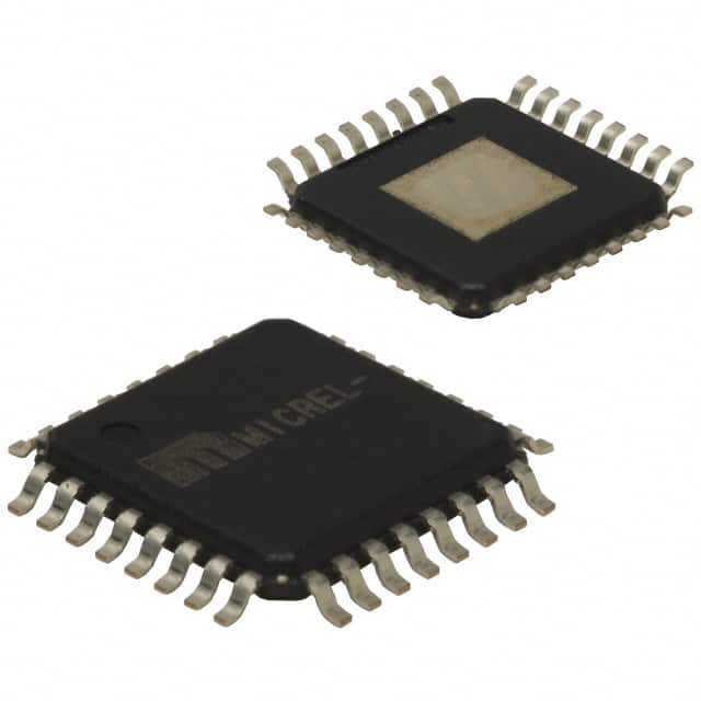
- Part No.:
- SY69753ALHG-TR
- Manufacturer:
- Microchip Technology
- Category:
- Application Specific Clock/Timing
- Package:
- 32-TQFP Exposed Pad
- Datasheet:
-
 SY69753ALHG-TR.pdf
- Description:
- IC CLK DATA REC SDH 155MBPS
- Quantity:
- Payment:

- Shipping:

Inventory:3,648
Please send an inquiry. Send us your inquiry, and we will respond immediately.
Product details
Overview
SY69753ALHG-TR from Micrel Inc. is a 3.3V clock and data recovery (CDR) IC for SONET/SDH OC-3/STS-3 systems, supporting 125Mbps and 155Mbps NRZ data streams with differential PECL I/O, on-chip dual PLL architecture, and link fault detection. It operates across –40°C to +85°C and delivers recovered clock (RCLK/TCLK) and retimed data (RDOUT) outputs with <±200ps skew and 45–55% duty cycle.
For engineers reviewing the SY69753ALHG-TR datasheet, SY69753ALHG-TR pinout, SY69753ALHG-TR application, or SY69753ALHG-TR equivalent, key selection criteria include its 125/155Mbps NRZ CDR capability, dual-PLL clock synthesis and recovery, industrial temperature range, 32-pin EPAD-TQFP package, and compatibility with SONET/SDH/ATM line interface designs requiring low-jitter clock alignment and loss-of-signal resilience.
Technical Context
The SY69753ALHG-TR implements two independent PLLs: one for frequency synthesis using REFCLK as reference (with selectable divide ratios of 8×, 10×, 16×, or 20×), and another for clock recovery synchronized directly to the RDINP/RDINN data stream. The VCO center frequency ranges from 720MHz to 1250MHz, with ±5% tolerance and 15µs acquisition lock time.
It features asynchronous LFIN output indicating PLL lock status (active HIGH when RDIN is within ±1000ppm of synthesizer frequency), carrier detect (CD)-controlled recovery mode switching, and integrated loop filter pins (PLLRN/PLLRP, PLLSP/PLLSN) for external RC tuning. All PECL I/O complies with ECL 100K levels, while TTL inputs/outputs meet standard 3.3V logic thresholds.
Key Specifications
| Parameter | Value and Actual Design Meaning |
|---|---|
| Supply Voltage | 3.15V to 3.45V - ensures stable operation under industrial rail tolerances and enables direct use with standard 3.3V LDOs. |
| Data Rate Support | 125Mbps / 155Mbps NRZ - matches OC-3/STS-3 line rates with full jitter tracking and 30µs continuous 1s/0s tolerance. |
| VCO Center Frequency | 720MHz to 1250MHz - provides precise clock generation aligned to byte-rate multiples for sampling integrity. |
| Recovered Clock Skew | ±200ps - guarantees tight timing margin between RCLK and RDOUT for reliable data capture in high-speed serial links. |
| Lock Acquisition Time | 15µs - enables rapid reacquisition after signal interruption, critical for SONET APS and hitless protection switching. |
| Operating Temperature | –40°C to +85°C - validated for deployment in uncontrolled telecom chassis environments without derating. |
| Power Supply Current | 120mA to 160mA - reflects low-power CDR design, consuming ~30% less than SY87701V at comparable data rates. |
Pinout & Package
SY69753ALHG-TR is housed in a 32-pin EPAD-TQFP (package code H32-1) with exposed thermal pad for enhanced thermal dissipation in high-density line card layouts.
| Pin/Terminal | Circuit Role | Design Meaning |
|---|---|---|
| RDINP / RDINN | Differential PECL serial data input | Accepts AC- or DC-coupled NRZ data without external line receiver; drives internal receive PLL for clock recovery. |
| REFCLK | TTL reference clock input | Sets VCO center frequency via programmable divider; maintains clock stability during loss of RDIN signal. |
| CD | Carrier detect control input | Enables/disables CDR function: HIGH enables normal recovery; LOW forces RDOUT/LFIN LOW and locks PLL to REFCLK. |
| RDOUTP / RDOUTN | Differential PECL recovered data output | Retimed NRZ data aligned to rising edge of RCLK; meets ECL 100K specs for interfacing with downstream logic or serializers. |
| RCLKP / RCLKN | Differential PECL recovered clock output | Phase-aligned clock used to sample RDOUT; supports <±200ps skew and 45–55% duty cycle for robust eye opening. |
| TCLKP / TCLKN | Differential PECL selectable clock output | Outputs either RCLK (CLKSEL = HIGH) or synthesizer clock (CLKSEL = LOW); enables flexible clock routing in multi-channel systems. |
| LFIN | TTL link fault indicator output | Asynchronous active-HIGH signal confirms PLL lock to RDIN within ±1000ppm; toggles during unlock for diagnostics. |
| PLLRN / PLLRP | Receiver PLL loop filter terminals | Connect external RC network (R=680Ω, C=1.0µF) to tune bandwidth for SONET jitter compliance and transition density handling. |
| PLLSP / PLLSN | Synthesis PLL loop filter terminals | Connect external RC network (R=350Ω, C=1.0µF) to stabilize frequency multiplication and suppress reference clock phase noise. |
| DIVSEL1 / DIVSEL2 | TTL divider select inputs | Set fRCLK/fREFCLK ratio to 8, 10, 16, or 20 - determines output clock frequency based on reference source. |
| CLKSEL | TTL clock select input | Selects TCLK source: recovered clock (HIGH) or synthesized clock (LOW), enabling dual-clock domain support. |
| VCC / VCCA / VCCO | Power supply pins | All three must be tied to same 3.3V rail; VCCA powers analog PLL blocks, VCCO drives PECL outputs, ensuring noise isolation. |
Key Features
| Feature | Design Value |
|---|---|
| Dual independent PLLs | Separate clock synthesis (REFCLK-based) and clock recovery (RDIN-based) paths eliminate cross-talk and enable simultaneous reference holdover and data lock. |
| Link fault detection with LFIN | Asynchronous TTL output signals PLL lock status in real time, enabling automated system-level fault reporting and failover without host processor intervention. |
| Carrier detect (CD) control | Hardware-gated CDR enable/disable allows seamless integration with optical module CD signals, preventing false lock during initialization or fiber disconnect. |
| Industrial temperature range | Guaranteed operation from –40°C to +85°C supports deployment in outdoor cabinets, central office shelves, and uncooled line cards. |
| Low-power 3.3V design | 120–160mA ICC at 3.3V reduces thermal load and simplifies power delivery in multi-channel CDR applications compared to legacy 5V solutions. |
Applications
| SONET/SDH OC-3 Line Interface | Ethernet Media Converter |
|---|---|
|
Use Scenario: Aggregating DS3/E3 tributaries into OC-3 framed traffic for transport over fiber. IC Role / Device Role / Timing Role: Performs clock recovery and data retiming on incoming OC-3 payload, extracting embedded clock and aligning data to local timing domain. Use Value: Enables deterministic jitter transfer (<1 UI peak-to-peak) and maintains frame synchronization during pointer adjustments and AIS insertion. |
Use Scenario: Converting 100BASE-FX fiber signals to 100BASE-TX copper links in enterprise edge switches. IC Role / Device Role / Timing Role: Recovers clock and retimes data from 125Mbps NRZ fiber stream, providing clean, low-skew clock and data for PHY interface. Use Value: Eliminates need for external line receivers and clock cleaners, reducing BOM count and board area in compact media converter modules. |
| Proprietary 120–180Mbps Serial Link | ATM Cell Transport Interface |
|
Use Scenario: High-reliability backplane interconnect between FPGA-based packet processors in military comms equipment. IC Role / Device Role / Timing Role: Provides jitter-tolerant clock recovery and data retiming for custom NRZ protocols operating near 155Mbps. Use Value: Supports continuous 1s/0s sequences up to 30µs, meeting MIL-STD-810G thermal cycling and EMI resilience requirements. |
Use Scenario: ATM layer 1 framing in DSLAM line cards handling UBR/CBR traffic over OC-3 physical layer. IC Role / Device Role / Timing Role: Recovers cell delineation clock and retimes ATM cell payloads for SAR processing and QoS scheduling. Use Value: Maintains cell timing accuracy under bursty traffic and transient LOS conditions via REFCLK holdover and LFIN-driven alarm assertion. |
Equivalent & Alternatives
The following parts are listed as comparable options for similar clock and data recovery applications.
| Alternative Part | Technical Difference | Application Difference | Selection Advice |
|---|---|---|---|
| SY87701AL | Wider rate range (28–1300Mbps), single PLL architecture, higher power consumption (~30% more than SY69753ALHG-TR). | Supports AnyRate® operation across multiple standards (e.g., Fibre Channel, GigE), not optimized for fixed OC-3 lock-in. | Choose SY87701AL only if multi-standard flexibility and variable-rate adaptation outweigh fixed-rate efficiency and lower power. |
| ICS87301AGI | Single PLL CDR, 155Mbps-only, no REFCLK holdover mode, lacks CD input and LFIN output. | Designed for simpler point-to-point links without SONET-compliant fault signaling or carrier-controlled recovery gating. | Choose ICS87301AGI only for cost-sensitive, non-SONET applications where link monitoring and holdover are unnecessary. |
Compared with SY87701AL and ICS87301AGI, the SY69753ALHG-TR uniquely combines dual-PLL architecture, REFCLK holdover, carrier detect control, and SONET-specific lock detection-making it the only option among the three qualified for OC-3 line interface designs requiring guaranteed jitter performance and loss-of-signal resilience.
Availability
SY69753ALHG-TR is available at Aetrix Electronics and suitable for SONET/SDH OC-3 line interfaces, Ethernet media converters, and proprietary 120–180Mbps serial links requiring stable component supply, long-term lifecycle assurance, and traceable sourcing.
Supply support for SY69753ALHG-TR includes scheduled delivery planning, volume procurement assistance, BOM continuity management, traceable sourcing, and lifecycle availability coordination for OEM customers, industrial embedded developers, connected-device designers, and electronics production programs.
Manufacturer
Micrel Inc. was a fabless semiconductor company specializing in high-performance analog, RF, and timing solutions before its acquisition by Microchip Technology in 2015. It pioneered low-power, high-speed CDR and clock management ICs for telecom infrastructure.
The SY69753ALHG-TR belongs to Micrel's SY69xxx family of SONET/SDH-compliant clock recovery ICs, designed specifically for OC-3/STS-3 line interface applications demanding deterministic jitter handling, industrial temperature operation, and integrated fault monitoring.
FAQ
What data rates does the SY69753ALHG-TR support?
The SY69753ALHG-TR supports 125Mbps and 155Mbps NRZ data streams, matching OC-3/STS-3 line rates. Its dual-PLL architecture and VCO range (720–1250MHz) are optimized for these fixed rates-not variable-rate operation. The device achieves full jitter tracking and maintains lock under ±1000ppm frequency deviation, making it unsuitable for broader AnyRate® applications.
How does the SY69753ALHG-TR handle loss of input signal?
When RDIN is lost, the SY69753ALHG-TR uses the REFCLK input to maintain clock output stability. The CD input controls this behavior: with CD HIGH, the receiver PLL attempts lock to RDIN; with CD LOW, the PLL locks exclusively to REFCLK, forcing RDOUT and LFIN LOW. This holdover mode ensures continuous clock output without interruption, critical for SONET hitless protection switching.
What is the purpose of the LFIN output on the SY69753ALHG-TR?
The LFIN output on the SY69753ALHG-TR is an asynchronous TTL signal indicating PLL lock status. It goes HIGH when the receiver PLL is locked to RDIN within ±1000ppm and toggles when unlocked. Unlike a simple lock detect, LFIN remains active during valid data reception and provides real-time diagnostics for system-level fault reporting and automatic failover decisions.
Can the SY69753ALHG-TR generate both recovered and synthesized clocks simultaneously?
Yes-the SY69753ALHG-TR provides separate differential outputs: RCLKP/RCLKN carry the recovered clock, while TCLKP/TCLKN deliver either the recovered clock (when CLKSEL = HIGH) or the synthesized clock (when CLKSEL = LOW). This dual-clock capability enables flexible timing architectures, such as feeding recovered clock to data path and synthesized clock to control logic or parallel interfaces.
What external components are required for stable operation of the SY69753ALHG-TR?
The SY69753ALHG-TR requires two external RC loop filter networks: 680Ω + 1.0µF for the receiver PLL (PLLRN/PLLRP) and 350Ω + 1.0µF for the synthesis PLL (PLLSP/PLLSN). Additionally, proper 3.3V decoupling (0.1µF and 1.0µF ceramics near VCC/VCCA/VCCO pins) and 50Ω termination on all unused PECL outputs are mandatory for jitter performance and signal integrity.
SY69753ALHG-TR Specifications
- Product attributes
- Attribute value
- Manufacturer:
- Microchip Technology
- Series:
- -
- Package/Case:
- 32-TQFP Exposed Pad
- Packaging:
- Tape & Reel (TR)
- Product Status:
- Active
- Programmable:
- Not Verified
- PLL:
- Yes
- Main Purpose:
- Ethernet, SONET/SDH, ATM OC-3
- Input:
- PECL
- Output:
- PECL
- Number of Circuits:
- 1
- Ratio - Input:Output:
- 1:3
- Differential - Input:Output:
- Yes/Yes
- Frequency - Max:
- 155Mbps
- Voltage - Supply:
- 3.15V ~ 3.45V
- Operating Temperature:
- -40°C ~ 85°C
- Mounting Type:
- Surface Mount
- Grade:
- -
- Qualification:
- -
- Supplier Device Package:
- 32-TQFP-EP (7x7)
SY69753ALHG-TR FAQ
1.How can I place an order for SY69753ALHG-TR through Aetrix?
Please submit a Request for Quotation (RFQ) for SY69753ALHG-TR on Aetrix. Our sales agent will provide a competitive quotation and guide you through the order confirmation once you accept the terms.
2.Are the price and stock information for SY69753ALHG-TR reliable?
The price and inventory of SY69753ALHG-TR are updated periodically and may fluctuate due to market conditions. Stock and pricing data are typically refreshed every 24 hours. Quotation validity for SY69753ALHG-TR is usually 5 days.
3.What payment methods are accepted for SY69753ALHG-TR?
We accept Wire Transfer, PayPal, Credit Card, Western Union, MoneyGram, and Escrow for SY69753ALHG-TR transactions.
Note: Certain payment methods may incur a processing fee.
4.How is shipping managed for SY69753ALHG-TR?
SY69753ALHG-TR orders can be shipped via leading logistics carriers, including DHL, UPS, FedEx, TNT, or Registered Mail.
Once your SY69753ALHG-TR order is processed, you will receive an email with the shipment details and tracking number.
Note: Tracking information may take up to 24 hours to appear. Express delivery typically takes 3–5 business days.
5.How can I obtain technical support or documentation for SY69753ALHG-TR?
For technical support, including SY69753ALHG-TR datasheets, pinout diagrams, or application guidance, please contact our engineering support team. They can provide detailed documentation and assistance for your SY69753ALHG-TR requirements.
6.How does Aetrix verify that SY69753ALHG-TR is sourced from the original manufacturer or authorized distributors?
All SY69753ALHG-TR products on Aetrix are procured from qualified distributors and authorized channels. Our dedicated quality assurance team conducts strict verification, including traceability checks and, if necessary, third-party testing. This ensures that SY69753ALHG-TR meets industry standards.
7.What is the process for return or replacement of SY69753ALHG-TR?
All SY69753ALHG-TR units undergo pre-shipment inspection (PSI). If there is an issue with SY69753ALHG-TR, returns or replacements are accepted under the following conditions:
1.Quantity discrepancies, incorrect items, or visible external defects (such as breakage or corrosion), acknowledged by Aetrix.
2.The issue is reported within 90 days of delivery.
3.The SY69753ALHG-TR part is unused and in its original packaging.
Return procedure for SY69753ALHG-TR:
1.Submit a request within 90 days.
2.Obtain a Return Material Authorization (RMA) from Aetrix.
SY69753ALHG-TR Tags
-
LMK00334RTVRQ1
Texas Instruments
.jpg)
-
DSC557-0344FI0T
Microchip Technology
-
9FGV0241AKILFT
Renesas

-
9DBL0452CKILFT
Renesas
-
DSC557-0344FL1T
Microchip Technology
-
RC19008AGND#KB0
Renesas
-
RC19008AGND#BB0
Renesas

-
9DB403DGILFT
Renesas
-
9DB233AGILFT
Renesas

-
9DB803DGILFT
Renesas
-
9FGL0851DKILFT
Renesas
-
AB-557-03-HCHC-F-L-C-T
Abracon LLC
Tech Hub

TTL and CMOS logic families differ in thresholds, loading, output drive, power and timing. This engineering guide compares 74HC and 74HCT, calculates noise margins and checks 3.3 V/5 V compatibility.

A practical engineering guide to 3.3V and 5V logic compatibility, input thresholds, resistor dividers, translator ICs, MOSFET level shifting, I2C pull-ups, timing limits and power-sequencing risks.

The 74HC595 uses push-pull logic outputs, while the TPIC6B595 uses 50 V open-drain DMOS sinks for higher-power loads. This guide compares timing, current limits, 3.3 V interfacing, load wiring, thermal…

The 74HC595 converts serial data into eight stable parallel outputs. This guide covers pin functions, shift and storage timing, OE and MR behavior, drive-current limits, cascading, voltage compatibilit…

A technical comparison of level-sensitive latches and edge-triggered flip-flops, covering timing windows, setup and hold limits, master–slave operation, time borrowing, race-through, HDL inference and…

A D latch stores one bit while Enable controls when data can pass. This reference covers gate-level operation, truth tables, transparency, setup and hold timing, LE versus OE, common ICs and practical …

An SR latch stores one bit through cross-coupled feedback. This engineering reference covers NOR and NAND implementations, truth tables, forbidden-state recovery, gated operation, switch debouncing, fa…

Latch circuits retain one bit through feedback. This technical reference covers SR and D latches, truth tables, transparency, timing limits, latch-versus-flip-flop behavior, applications and common log…

An engineering guide to LED driver operation, constant-current and constant-voltage outputs, linear and switching topologies, dimming, IC selection, calculations, replacement compatibility, and fault c…

Operational amplifier guide covering op amp basics, feedback, ideal vs real op amps, common configurations, buffer circuits, offset, bias current, gain-bandwidth, slew rate, rail-to-rail limits and sel…


