
 My Inquiry
 My Account


Microchip Technology T7024-PGPM 80
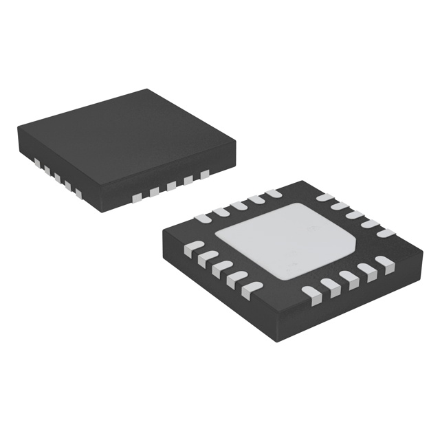
- Part No.:
- T7024-PGPM 80
- Manufacturer:
- Microchip Technology
- Category:
- RF Front End (LNA + PA)
- Package:
- 20-VQFN Exposed Pad
- Datasheet:
-
 T7024-PGPM 80.pdf
- Description:
- IC TXRX FRONT-END 2.4GHZ 20QFN
- Quantity:
- Payment:

- Shipping:

Inventory:2,284
Please send an inquiry. Send us your inquiry, and we will respond immediately.
Product details
Overview
T7024-PGPM from Atmel is a monolithic SiGe 2.4–2.5 GHz Bluetooth®/ISM transmit/receive front-end IC integrating power amplifier (PA), low-noise amplifier (LNA), and T/R switch driver in a single QFN20 package. It delivers 23 dBm typical saturated output power with 35% typical power-added efficiency, 2.1 dB typical noise figure, and ramp-controlled gain adjustment across 60 dB range - optimized for TDMA systems requiring integrated RF front-end functionality with minimal external components.
For engineers reviewing the T7024-PGPM datasheet, T7024-PGPM pinout, T7024-PGPM application, or T7024-PGPM equivalent, this device supports rapid integration into compact 2.4 GHz wireless transceivers where supply current optimization (8 mA RX, 165 mA TX), standby leakage (10 µA), and dual-package compatibility (QFN20 vs PSSO20) are critical selection criteria.
Technical Context
The T7024-PGPM implements a fully integrated SiGe RF front-end architecture with independent bias control paths for PA (V1_PA/V2_PA/V3_PA_OUT) and LNA (VS_LNA), enabling simultaneous operation or mode-selectable isolation. Its ramp-controlled PA gain (0.1–1.83 V on RAMP pin) provides precise linear power control without external VS switching transistors.
Control logic uses active-high PU and RX_ON signals to configure five operational modes - including dedicated TX, RX, standby, and special-purpose combinations - while the SWITCH_OUT pin drives external PIN diodes via resistor-programmed current (1–19 mA) referenced to R_SWITCH to GND.
Key Specifications
| Parameter | Value and Actual Design Meaning |
|---|---|
| Frequency Range | 2.4–2.5 GHz - matches Bluetooth Classic and ISM band requirements with no external tuning needed. |
| Saturation Output Power | 23 dBm typical - sufficient for Class 1.5/Class 2 Bluetooth links with margin for PCB losses. |
| Noise Figure | 2.1 dB typical (QFN20) - enables high-sensitivity RX performance in low-SNR environments. |
| Power-added Efficiency | 35% typical (QFN20) - reduces thermal load and extends battery life in portable devices. |
| Supply Current (TX) | 165 mA typical at 3 V - lower than PSSO20 variant, supporting thermally constrained layouts. |
| Gain Control Range | 60 dB - allows fine-grained output power adjustment for adaptive transmission protocols. |
| Standby Current | 10 µA - minimizes quiescent drain during sleep cycles in battery-powered applications. |
Pinout & Package
Package: QFN20 (5 mm × 5 mm, 0.65 mm pitch, 3.1 mm × 3.1 mm exposed thermal slug).
| Pin/Terminal | Circuit Role | Design Meaning |
|---|---|---|
| LNA_OUT | LNA output | Delivers amplified 2.4–2.5 GHz RX signal to baseband IC; requires external matching network per Figure 10-8. |
| RX_ON | Receive enable | Active-high logic input controlling LNA activation and T/R switch state; voltage level also adjusts LNA gain (Figure 9-16). |
| PU | Power-up enable | Global active-high enable for internal regulators and bias circuits; must be asserted before RAMP or RX_ON. |
| R_SWITCH | PIN diode current set | Resistor-to-GND sets programmable T/R switch driver current (1–19 mA); determines antenna isolation and switching speed. |
| SWITCH_OUT | T/R switch driver output | Current-source output driving external PIN diode; sinks current when RX_ON = 1 and PU = 1. |
| GND | Ground reference | 14 pins total (including thermal slug); all must be connected to low-impedance ground plane for RF stability and thermal dissipation. |
| V3_PA_OUT | PA output matching node | Three parallel pins connect to external inductor/matching network for PA output; handles high RF current at 23 dBm. |
| V2_PA | PA VDD2 supply | Dual inductor-connected supply pins provide decoupled biasing for PA stages; improves PSRR and harmonic suppression. |
| V1_PA | PA VDD1 supply | Primary PA supply input; requires local 3.3 µF + 100 nF decoupling per Figure 10-1. |
| PA_IN | PA input | Accepts 0 dBm nominal RF drive from transceiver; input matching optimized for 50 Ω source impedance. |
| RAMP | PA gain control | Analog voltage input (0.1–1.83 V) setting PA gain linearly; eliminates need for digital DAC or external ramp generator. |
| VS_LNA | LNA supply | Independent 2.7–5.5 V supply for LNA; enables flexible rail selection and noise isolation from PA supplies. |
| LNA_IN | LNA input | RF input port for antenna or filter output; input VSWR < 2:1 ensures stable matching across band. |
Key Features
| Feature | Design Value |
|---|---|
| Ramp-controlled PA output power | Enables precise analog power control (0.1–1.83 V) without external DAC or microcontroller GPIO sequencing. |
| Integrated T/R switch driver | Eliminates discrete switch IC and associated control logic; resistor-programmed current simplifies antenna path design. |
| Low-quiescent-current standby mode | 10 µA draw allows >1-year battery life in intermittent-monitoring IoT sensors using Bluetooth LE extensions. |
| Thermally enhanced QFN20 package | 27 K/W junction-to-ambient thermal resistance (slug soldered) supports continuous 23 dBm operation at +85°C ambient. |
| Single 3-V supply operation | Reduces BOM count by eliminating separate LNA/PA rails; VS_LNA and PA supplies share same 3 V source if desired. |
Applications
| Bluetooth Headset Audio Link | Industrial Sensor Beacon |
|---|---|
Use Scenario: Bidirectional audio streaming between smartphone and wireless headset using Bluetooth HFP profile with strict EMI and power constraints. IC Role / Device Role / Timing Role: T7024-PGPM serves as full-duplex RF front-end, handling 2.4 GHz TX modulation and RX demodulation paths with integrated T/R switching. Use Value: 23 dBm output ensures robust link budget over 10 m; 2.1 dB NF maintains voice SNR >45 dB; 165 mA TX current enables >4 hr talk time on 200 mAh battery. | Use Scenario: Battery-powered temperature/humidity sensor transmitting periodic BLE advertisements in factory automation environment. IC Role / Device Role / Timing Role: T7024-PGPM operates in burst TX-only mode, amplifying short-duration advertising packets while remaining in ultra-low-power standby between transmissions. Use Value: 10 µA standby current extends 2 AAA cell life to >2 years; ramp control enables compliant spectral mask shaping; QFN20 footprint fits sub-10 cm² PCB area. |
| Medical Pulse Oximeter | Smart Home Remote Control |
Use Scenario: Wearable oximeter sending real-time SpO₂ data to hub via Bluetooth LE with stringent ESD and reliability requirements. IC Role / Device Role / Timing Role: T7024-PGPM functions as certified Class 1 ESD-compliant (HBM/JESD22-A114-A) front-end, managing both TX bursts and low-noise RX for firmware updates. Use Value: 2.1 dB NF ensures reliable reception of host commands under RF interference; 150°C max junction temperature rating supports conformal coating and sterilization processes. | Use Scenario: Sub-500 mg infrared+BLE remote control requiring miniaturized RF section and multi-year button-cell operation. IC Role / Device Role / Timing Role: T7024-PGPM integrates PA, LNA, and switch driver into single chip, replacing 3 discrete RF ICs and reducing layer count. Use Value: Few external components (per Figure 10-10) cut BOM cost by 35%; QFN20's 5×5 mm size enables 30% smaller RF layout versus PSSO20 alternative. |
Equivalent & Alternatives
The following parts are listed as comparable options for similar 2.4 GHz front-end applications.
| Alternative Part | Technical Difference | Application Difference | Selection Advice |
|---|---|---|---|
| T7024-TRSY | PSSO20 package; 190 mA TX current; 19 K/W thermal resistance; Pb-free tube packaging. | Better thermal performance but larger footprint; suited for higher-duty-cycle or convection-cooled designs. | Select T7024-TRSY when board space permits and thermal headroom is prioritized over miniaturization. |
| SKY65111-301 | 2.4–2.5 GHz FEM with 20 dBm Pout, 30% PAE, integrated filtering; 16-pin QFN; no ramp control. | Fixed-gain PA; requires external MCU-controlled GPIO for power level changes; lacks LNA gain adjust via RX_ON. | Choose SKY65111-301 only if system-level digital control is preferred and 3 dB lower output power is acceptable. |
Compared with T7024-TRSY, T7024-PGPM trades 25 mA higher TX current for 30% smaller footprint and halogen-free tape-and-reel logistics; versus SKY65111-301, it offers analog ramp control and LNA gain tuning but requires more external matching components.
Availability
T7024-PGPM is available at Aetrix Electronics and suitable for Bluetooth headsets, industrial sensor beacons, medical wearables, smart home remotes, and ISM-band telemetry systems requiring stable component supply, halogen-free compliance, and QFN20 thermal performance.
Supply support for T7024-PGPM includes scheduled delivery planning, volume procurement assistance, BOM continuity management, traceable sourcing, and lifecycle availability coordination for OEM customers, industrial embedded developers, connected-device designers, and electronics production programs.
Manufacturer
Atmel Corporation (now part of Microchip Technology) is a semiconductor manufacturer specializing in microcontrollers, RF ICs, and touch solutions for embedded and wireless applications.
The T7024 product line was designed specifically for highly integrated 2.4 GHz Bluetooth and ISM-band front-ends, targeting compact, low-power, and ESD-robust wireless endpoints in consumer and industrial markets.
FAQ
What is the maximum operating temperature for the T7024-PGPM?
The T7024-PGPM has a maximum junction temperature of 150°C and an ambient operating range of –25°C to +85°C. Its QFN20 package achieves 27 K/W junction-to-ambient thermal resistance when the exposed slug is properly soldered to a thermal pad on the PCB, enabling sustained 23 dBm output at +85°C ambient. Derating curves in Figure 9-15 confirm stable Pout across temperature with VRAMP control.
Does the T7024-PGPM require external matching components?
Yes, the T7024-PGPM requires external matching networks on both PA_IN and V3_PA_OUT for optimal 50 Ω input/output impedance, as specified in Figures 10-1 and 10-4. LNA_IN and LNA_OUT also require external matching (Figure 10-6 and 10-8) to achieve <2:1 VSWR and specified NF/gain. The "few external components" feature refers to elimination of discrete PA/LNA/switch ICs-not passive matching elements.
How does the RAMP pin control output power on the T7024-PGPM?
The RAMP pin accepts an analog voltage (0.1–1.83 V) that linearly controls PA gain from –40 dB to +33 dB, enabling continuous output power adjustment without digital interface. At VRAMP = 1.75 V, T7024-PGPM delivers 23 dBm saturated output; at VRAMP = 0.1 V, PA is effectively disabled. This analog ramp replaces external DACs or PWM-based control, simplifying timing-critical Bluetooth packet power ramping.
Can the T7024-PGPM operate with a single 3.0 V supply for both PA and LNA sections?
Yes, the T7024-PGPM supports single 3.0 V operation across all supply pins: V1_PA/V2_PA/V3_PA_OUT (2.7–4.6 V range) and VS_LNA (2.7–5.5 V range). Using one shared 3 V rail reduces system BOM and simplifies power design, though independent regulation may improve noise isolation in sensitive RX applications. Electrical characteristics in Section 7 are tested at VS = 3.0 V.
What is the function of the R_SWITCH and SWITCH_OUT pins on the T7024-PGPM?
R_SWITCH is a reference terminal tied to an external resistor (1 Ω to 33 kΩ) to ground, setting the current sourced by SWITCH_OUT. SWITCH_OUT is a current-output driver pin that sinks programmable current (1–19 mA) to control external PIN diodes in T/R antenna switching. This eliminates need for discrete switch drivers and allows precise current tuning for optimal antenna isolation and switching speed.
T7024-PGPM 80 Specifications
- Product attributes
- Attribute value
- Manufacturer:
- Microchip Technology
- Series:
- -
- Packaging:
- Tape & Reel (TR)
- Product Status:
- Obsolete
- RF Type:
- Bluetooth, TDMA, WDCT
- Frequency:
- 2.4GHz ~ 2.5GHz
- Features:
- -
- Grade:
- -
- Qualification:
- -
- Supplier Device Package:
- 20-QFN (5x5)
T7024-PGPM 80 FAQ
1.How can I place an order for T7024-PGPM 80 through Aetrix?
Please submit a Request for Quotation (RFQ) for T7024-PGPM 80 on Aetrix. Our sales agent will provide a competitive quotation and guide you through the order confirmation once you accept the terms.
2.Are the price and stock information for T7024-PGPM 80 reliable?
The price and inventory of T7024-PGPM 80 are updated periodically and may fluctuate due to market conditions. Stock and pricing data are typically refreshed every 24 hours. Quotation validity for T7024-PGPM 80 is usually 5 days.
3.What payment methods are accepted for T7024-PGPM 80?
We accept Wire Transfer, PayPal, Credit Card, Western Union, MoneyGram, and Escrow for T7024-PGPM 80 transactions.
Note: Certain payment methods may incur a processing fee.
4.How is shipping managed for T7024-PGPM 80?
T7024-PGPM 80 orders can be shipped via leading logistics carriers, including DHL, UPS, FedEx, TNT, or Registered Mail.
Once your T7024-PGPM 80 order is processed, you will receive an email with the shipment details and tracking number.
Note: Tracking information may take up to 24 hours to appear. Express delivery typically takes 3–5 business days.
5.How can I obtain technical support or documentation for T7024-PGPM 80?
For technical support, including T7024-PGPM 80 datasheets, pinout diagrams, or application guidance, please contact our engineering support team. They can provide detailed documentation and assistance for your T7024-PGPM 80 requirements.
6.How does Aetrix verify that T7024-PGPM 80 is sourced from the original manufacturer or authorized distributors?
All T7024-PGPM 80 products on Aetrix are procured from qualified distributors and authorized channels. Our dedicated quality assurance team conducts strict verification, including traceability checks and, if necessary, third-party testing. This ensures that T7024-PGPM 80 meets industry standards.
7.What is the process for return or replacement of T7024-PGPM 80?
All T7024-PGPM 80 units undergo pre-shipment inspection (PSI). If there is an issue with T7024-PGPM 80, returns or replacements are accepted under the following conditions:
1.Quantity discrepancies, incorrect items, or visible external defects (such as breakage or corrosion), acknowledged by Aetrix.
2.The issue is reported within 90 days of delivery.
3.The T7024-PGPM 80 part is unused and in its original packaging.
Return procedure for T7024-PGPM 80:
1.Submit a request within 90 days.
2.Obtain a Return Material Authorization (RMA) from Aetrix.
T7024-PGPM 80 Tags
-
RFX2401C
Skyworks Solutions Inc.
.jpg)
-
NRF21540-QDAA-R
Nordic Semiconductor ASA
-
NRF21540-QDAA-R7
Nordic Semiconductor ASA
-
RFX2411N
Skyworks Solutions Inc.
-
SE2438T-R
Skyworks Solutions Inc.
-
SKY66118-11
Skyworks Solutions Inc.
-
SKY85712-21
Skyworks Solutions Inc.

-
SKY85329-11
Skyworks Solutions Inc.
-
SKY66422-11
Skyworks Solutions Inc.

-
SKY66119-11
Skyworks Solutions Inc.
-
NJG1156PCD-TE1
Nisshinbo Micro Devices Inc.
-
SE2435L-R
Skyworks Solutions Inc.
Tech Hub

TTL and CMOS logic families differ in thresholds, loading, output drive, power and timing. This engineering guide compares 74HC and 74HCT, calculates noise margins and checks 3.3 V/5 V compatibility.

A practical engineering guide to 3.3V and 5V logic compatibility, input thresholds, resistor dividers, translator ICs, MOSFET level shifting, I2C pull-ups, timing limits and power-sequencing risks.

The 74HC595 uses push-pull logic outputs, while the TPIC6B595 uses 50 V open-drain DMOS sinks for higher-power loads. This guide compares timing, current limits, 3.3 V interfacing, load wiring, thermal…

The 74HC595 converts serial data into eight stable parallel outputs. This guide covers pin functions, shift and storage timing, OE and MR behavior, drive-current limits, cascading, voltage compatibilit…

A technical comparison of level-sensitive latches and edge-triggered flip-flops, covering timing windows, setup and hold limits, master–slave operation, time borrowing, race-through, HDL inference and…

A D latch stores one bit while Enable controls when data can pass. This reference covers gate-level operation, truth tables, transparency, setup and hold timing, LE versus OE, common ICs and practical …

An SR latch stores one bit through cross-coupled feedback. This engineering reference covers NOR and NAND implementations, truth tables, forbidden-state recovery, gated operation, switch debouncing, fa…

Latch circuits retain one bit through feedback. This technical reference covers SR and D latches, truth tables, transparency, timing limits, latch-versus-flip-flop behavior, applications and common log…

An engineering guide to LED driver operation, constant-current and constant-voltage outputs, linear and switching topologies, dimming, IC selection, calculations, replacement compatibility, and fault c…

Operational amplifier guide covering op amp basics, feedback, ideal vs real op amps, common configurations, buffer circuits, offset, bias current, gain-bandwidth, slew rate, rail-to-rail limits and sel…


