
 My Inquiry
 My Account


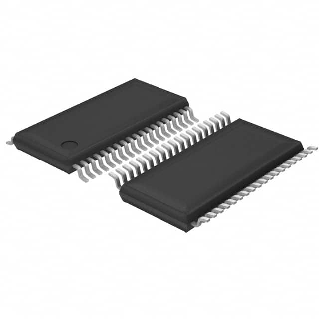
Texas Instruments TAS5086DBT
- Part No.:
- TAS5086DBT
- Manufacturer:
- Texas Instruments
- Category:
- Audio Special Purpose
- Package:
- 38-TFSOP (0.173", 4.40mm Width)
- Datasheet:
-
 TAS5086DBT.pdf
- Description:
- IC MODULATOR 38TSSOP
- Quantity:
- Payment:

- Shipping:

Inventory:1,418
Please send an inquiry. Send us your inquiry, and we will respond immediately.
Product details
Overview
TAS5086DBT from Texas Instruments is a six-channel digital pulse-width modulator (PWM) IC designed for high-fidelity audio systems. It accepts 16-/20-/24-bit I2S, left-justified, or right-justified serial audio inputs at sampling rates from 32 kHz to 192 kHz, performs 8× oversampling with fourth-order noise shaping, delivers ≥105-dB dynamic range (20 Hz–20 kHz), and outputs six PWM channels compatible with single-ended or bridge-tied load power stages - used in home theater AV receivers and multi-channel active speaker systems.
For engineers reviewing the TAS5086DBT datasheet, TAS5086DBT pinout, TAS5086DBT application, or TAS5086DBT equivalent, key selection considerations include its 38-pin TSSOP package, I2C slave control interface (100/400 kHz), 3.3-V-only digital/analog supply, 64-/48-fS bit-clock support, and AM interference avoidance capability via adjustable PWM clock rate.
Technical Context
The TAS5086DBT operates as a clock-slave device requiring external MCLK, SCLK, and LRCLK; it auto-detects input sample rates (32/44.1/48/88.2/96/176.4/192 kHz) and supports 128–512-fS master clock rates up to 50 MHz. Its PLL uses internal oscillator trim (via OSC_RES) for stability without external crystal.
It implements a 1N+1 PWM signaling interface (six independent PWM outputs + one VALID2 sync signal), supports full channel remapping, integrates two programmable biquads in the subwoofer channel for bass management, and provides soft-mute, soft-start/stop, and intelligent AM interference avoidance by dynamically adjusting modulation clock rates to suppress RF coupling.
Key Specifications
| Parameter | Value and Actual Design Meaning |
|---|---|
| Channels | Six independent PWM output channels with full input-to-output mapping flexibility |
| Sampling Rates | Supports 32, 44.1, 48, 88.2, 96, 176.4, and 192 kHz - auto-detected or manually set |
| Oversampling | 12× at 32 kHz; 8× at 44.1/48 kHz; 4× at 88.2/96 kHz; 2× at 176.4/192 kHz |
| Dynamic Range | ≥105 dB (20 Hz–20 kHz, measured with TAS5186 back-end) |
| THD+N | <0.06% (measured at TAS5086DBT PWM outputs, not speaker terminals) |
| Supply Voltage | DVDD = AVDD = 3.0–3.6 V - single 3.3-V rail powers both digital and analog sections |
| I²C Interface | Standard/fast-mode slave (100/400 kHz); operates without MCLK present |
| Package | 38-pin TSSOP (DBT) with exposed thermal pad - RoHS-compliant, lead-free |
Pinout & Package
38-pin TSSOP (DBT) package with thermal pad; requires 0.1-µF low-ESR decoupling on VR_ANA, VR_DIG, and VR_OSC pins referenced to respective ground planes (AVSS, DVSS, AVSS_PLL).
| Pin/Terminal | Circuit Role | Design Meaning |
|---|---|---|
| PWM_1 to PWM_6 (Pins 33–38) | Digital PWM output | Direct drive signals for six-channel Class-D power stage; each independently mappable to any input channel |
| VALID1 / VALID2 (Pins 31–32) | Output validity indicator | VALID1 confirms soft-start completion; VALID2 indicates stable PWM output readiness - used for sequenced power-stage enable |
| SDIN1–SDIN4 (Pins 23–26) | Serial audio input | Four independent 24-bit serial ports supporting I2S/left/right-justified formats; SDIN4 selectable as pass-through to SDOUT |
| SDOUT (Pin 22) | I²S serial audio output | Fixed 24-bit I²S stereo output derived from downmix or SDIN4 - no I²C control, always active |
| MCLK / SCLK / LRCLK (Pins 8, 20, 19) | Timing reference inputs | Asynchronous clock inputs - MCLK up to 50 MHz; SCLK = 64-fS (all rates) or 48-fS (192/384-fS MCLK); LRCLK = 1-fS |
| SDA / SCL (Pins 17–18) | I²C control interface | 5-V-tolerant bidirectional data/clock lines - supports standard/fast-mode operation even without MCLK |
| PDN / RESET / MUTE (Pins 10, 9, 16) | System control inputs | Active-low PDN enables 100-ms soft power-down; RESET forces hard-mute and register reset; MUTE enables noiseless volume ramp |
| VR_ANA / VR_DIG / VR_OSC (Pins 1, 30, 15) | Internal voltage references | 1.8-V analog/digital/oscillator reference outputs - require local 0.1-µF low-ESR bypass to respective grounds |
Key Features
| Feature | Design Value |
|---|---|
| AM Interference Avoidance | Adjusts PWM clock rate to 7-/8-/9-fS to eliminate audible AM radio band interference without external components |
| Click-and-Pop Suppression | Optimized PWM startup/shutdown sequence eliminates audible transients - no external mute circuitry required |
| Subwoofer Channel Processing | Two programmable biquad filters (gain-compensated + low-pass) dedicated to channel 6 for bass management |
| Flexible Downmixing | 5.1-channel input can be downmixed to 2.1 or 3.1 outputs - result routed to front, center, or subwoofer channels |
| DC Blocking & De-emphasis | Per-channel DC blocking enabled by default; selectable 32/44.1/48-kHz de-emphasis filters per channel |
| AC-Coupling Capacitor Charging | Optimized PWM sequence pre-charges AC-coupling caps in single-ended configurations - prevents turn-on thump |
Applications
| Home Theater AV Receiver | Multi-Channel Active Speaker |
|---|---|
Use Scenario: 5.1 or 7.1 surround sound decoding and amplification in compact consumer AV receivers. IC Role / Device Role / Timing Role: Six-channel PWM processor receiving decoded PCM from DSP/MPEG decoder; generates synchronized PWM streams for discrete Class-D amplifier stages. Use Value: Enables high-efficiency, low-heat, high-SNR multi-channel audio with integrated bass management and AM-noise immunity - eliminating need for external clock synthesis or RF shielding. |
Use Scenario: Integrated powered loudspeaker with built-in 6-channel amplification and digital crossover. IC Role / Device Role / Timing Role: Central PWM engine driving six independent amplifier channels; accepts I²S from DSP or Bluetooth audio SoC. Use Value: Delivers ≥105-dB dynamic range and <0.06% THD+N at amplifier input stage while supporting flexible channel routing and subwoofer-specific biquad filtering. |
| Automotive Infotainment Head Unit | Professional Audio Monitor |
Use Scenario: High-fidelity cabin audio system with 6-speaker configuration and parametric EQ. IC Role / Device Role / Timing Role: Digital audio interface between SoC and Class-D amplifier array; handles sample-rate conversion and channel remapping. Use Value: Supports 192-kHz input with 2× oversampling and intelligent AM avoidance - critical for vehicle RF-noise environments without added shielding cost. |
Use Scenario: Studio-grade near-field monitor with active 3-way design (LF/MF/HF) and digital input. IC Role / Device Role / Timing Role: Precision PWM generator feeding three independent amplifier modules; uses SDOUT for loopback monitoring. Use Value: Provides flat 20-Hz–20-kHz noise floor and 48-dB volume control range - enabling accurate level matching and reference-level playback calibration. |
Equivalent & Alternatives
The following parts are listed as comparable options for similar six-channel digital PWM processor applications.
| Alternative Part | Technical Difference | Application Difference | Selection Advice |
|---|---|---|---|
| TAS5086PAP | 64-pin HTQFP package with enhanced thermal performance; identical electrical specs and register map | Better suited for high-power designs requiring >1 W dissipation; larger PCB footprint and reflow profile | Select TAS5086PAP when thermal margin is constrained or board layout allows QFP; TAS5086DBT preferred for space-constrained TSSOP designs |
| TAS5086DBTR | Same 38-pin TSSOP package but tape-and-reel packaging; identical die and electrical behavior | No functional difference - only packaging format differs (reel vs. tube); same pinout and thermal characteristics | TAS5086DBTR is drop-in compatible for automated assembly; TAS5086DBT is tube-packaged for prototyping and low-volume use |
Compared with TAS5086PAP and TAS5086DBTR, the TAS5086DBT offers identical PWM processing capability and feature set in the smallest surface-mount footprint, making it optimal for compact consumer audio products where board area and thermal mass are tightly constrained.
Availability
TAS5086DBT is available at Aetrix Electronics and suitable for home theater receivers, active speaker systems, automotive infotainment head units, and professional audio monitors requiring stable component supply across production lifecycles.
Supply support for TAS5086DBT includes scheduled delivery planning, volume procurement assistance, BOM continuity management, traceable sourcing, and lifecycle availability coordination for OEM customers, industrial embedded developers, connected-device designers, and electronics production programs.
Manufacturer
Texas Instruments is a global semiconductor leader specializing in analog, embedded processing, and digital signal technologies - serving industrial, automotive, and consumer markets with high-reliability silicon solutions.
The TAS5086DBT belongs to TI's PurePath Digital™ audio processor family, engineered specifically for high-efficiency, low-noise Class-D amplifier systems requiring precise PWM timing, advanced noise shaping, and seamless integration with digital audio sources.
FAQ
What is the maximum sampling rate supported by the TAS5086DBT?
The TAS5086DBT supports input sampling rates up to 192 kHz. At this rate, it applies 2× oversampling with fourth-order noise shaping to maintain ≥105-dB dynamic range across the 20 Hz–20 kHz audio band. The device auto-detects the rate or allows manual configuration via I²C registers, and accepts corresponding MCLK frequencies up to 50 MHz.
Does the TAS5086DBT require an external crystal or oscillator?
No, the TAS5086DBT does not require an external crystal. It uses an internal oscillator with external trim resistor (OSC_RES on Pin 14) for PLL reference. After power-up or reset, oscillator trim must be performed using the Oscillator Trim Register (0x1B) - eliminating BOM cost and board space for external timing components.
Can the TAS5086DBT drive both single-ended and bridge-tied load amplifiers?
Yes, the TAS5086DBT is explicitly designed to drive both configurations. Its six PWM outputs support 1N+1 signaling (six PWMs + one VALID2 sync signal) and are compatible with TI's TAS5186 (BTL/SE), TAS5142 (BTL/SE), and TAS5111/12 (with minimal external logic). The IC includes optimized PWM sequences for charging AC-coupling capacitors in single-ended setups.
How does the AM interference avoidance feature work in the TAS5086DBT?
The TAS5086DBT avoids AM radio band interference by dynamically adjusting its PWM clock rate to 7-fS, 8-fS, or 9-fS - shifting switching noise away from 530–1710 kHz. This occurs in concert with the sample-rate converter and requires manual sample-rate setting when enabled. No external components or layout changes are needed to activate this feature.
Is the TAS5086DBT pin-compatible with other devices in the TAS5086 family?
Yes, the TAS5086DBT shares identical pinout, register map, and electrical specifications with the TAS5086PAP (HTQFP) and TAS5086DBTR (tape-and-reel TSSOP). The only differences are package type (TSSOP vs. HTQFP) and packaging format (tube vs. reel); all three variants are functionally interchangeable in the same PCB footprint when using the DBT variant.
TAS5086DBT Specifications
- Product attributes
- Attribute value
- Manufacturer:
- Texas Instruments
- Series:
- PurePath Digital™
- Package/Case:
- 38-TFSOP (0.173", 4.40mm Width)
- Packaging:
- Bulk
- Product Status:
- Active
- Function:
- Modulator
- Applications:
- Digital Audio Interfacing
- Number of Channels:
- 6
- Interface:
- I2C, I2S
- Voltage - Supply:
- 3V ~ 3.6V
- Operating Temperature:
- 0°C ~ 70°C (TA)
- Specifications:
- 32kHz ~ 192kHz
- Mounting Type:
- Surface Mount
- Grade:
- -
TAS5086DBT FAQ
1.How can I place an order for TAS5086DBT through Aetrix?
Please submit a Request for Quotation (RFQ) for TAS5086DBT on Aetrix. Our sales agent will provide a competitive quotation and guide you through the order confirmation once you accept the terms.
2.Are the price and stock information for TAS5086DBT reliable?
The price and inventory of TAS5086DBT are updated periodically and may fluctuate due to market conditions. Stock and pricing data are typically refreshed every 24 hours. Quotation validity for TAS5086DBT is usually 5 days.
3.What payment methods are accepted for TAS5086DBT?
We accept Wire Transfer, PayPal, Credit Card, Western Union, MoneyGram, and Escrow for TAS5086DBT transactions.
Note: Certain payment methods may incur a processing fee.
4.How is shipping managed for TAS5086DBT?
TAS5086DBT orders can be shipped via leading logistics carriers, including DHL, UPS, FedEx, TNT, or Registered Mail.
Once your TAS5086DBT order is processed, you will receive an email with the shipment details and tracking number.
Note: Tracking information may take up to 24 hours to appear. Express delivery typically takes 3–5 business days.
5.How can I obtain technical support or documentation for TAS5086DBT?
For technical support, including TAS5086DBT datasheets, pinout diagrams, or application guidance, please contact our engineering support team. They can provide detailed documentation and assistance for your TAS5086DBT requirements.
6.How does Aetrix verify that TAS5086DBT is sourced from the original manufacturer or authorized distributors?
All TAS5086DBT products on Aetrix are procured from qualified distributors and authorized channels. Our dedicated quality assurance team conducts strict verification, including traceability checks and, if necessary, third-party testing. This ensures that TAS5086DBT meets industry standards.
7.What is the process for return or replacement of TAS5086DBT?
All TAS5086DBT units undergo pre-shipment inspection (PSI). If there is an issue with TAS5086DBT, returns or replacements are accepted under the following conditions:
1.Quantity discrepancies, incorrect items, or visible external defects (such as breakage or corrosion), acknowledged by Aetrix.
2.The issue is reported within 90 days of delivery.
3.The TAS5086DBT part is unused and in its original packaging.
Return procedure for TAS5086DBT:
1.Submit a request within 90 days.
2.Obtain a Return Material Authorization (RMA) from Aetrix.
TAS5086DBT Tags

-
SA571DR2G
onsemi
-
ADAU7002ACBZ-R7
Analog Devices Inc.

-
DRV135UA/2K5
Texas Instruments

-
DRV134UA/1K
Texas Instruments

-
DRV134PA
Texas Instruments
-
DRV134UA
Texas Instruments
-
DRV135UA
Texas Instruments
-
SA572DR2G
onsemi
-
PGA2311U/1K
Texas Instruments
-
SI8244BB-D-IS1R
Skyworks Solutions Inc.

-
CS8416K-CZZR
Cirrus Logic Inc.
-
SRC4392IPFBR
Texas Instruments
Tech Hub

A practical engineering guide to 3.3V and 5V logic compatibility, input thresholds, resistor dividers, translator ICs, MOSFET level shifting, I2C pull-ups, timing limits and power-sequencing risks.

The 74HC595 uses push-pull logic outputs, while the TPIC6B595 uses 50 V open-drain DMOS sinks for higher-power loads. This guide compares timing, current limits, 3.3 V interfacing, load wiring, thermal…

The 74HC595 converts serial data into eight stable parallel outputs. This guide covers pin functions, shift and storage timing, OE and MR behavior, drive-current limits, cascading, voltage compatibilit…

A technical comparison of level-sensitive latches and edge-triggered flip-flops, covering timing windows, setup and hold limits, master–slave operation, time borrowing, race-through, HDL inference and…

A D latch stores one bit while Enable controls when data can pass. This reference covers gate-level operation, truth tables, transparency, setup and hold timing, LE versus OE, common ICs and practical …

An SR latch stores one bit through cross-coupled feedback. This engineering reference covers NOR and NAND implementations, truth tables, forbidden-state recovery, gated operation, switch debouncing, fa…

Latch circuits retain one bit through feedback. This technical reference covers SR and D latches, truth tables, transparency, timing limits, latch-versus-flip-flop behavior, applications and common log…

An engineering guide to LED driver operation, constant-current and constant-voltage outputs, linear and switching topologies, dimming, IC selection, calculations, replacement compatibility, and fault c…

Operational amplifier guide covering op amp basics, feedback, ideal vs real op amps, common configurations, buffer circuits, offset, bias current, gain-bandwidth, slew rate, rail-to-rail limits and sel…

Jumper cables guide covering safe connection order, red and black clamp placement, final ground connection, cable gauge, length, clamp quality, copper vs CCA cables, jump starter comparison and battery…


