
 My Inquiry
 My Account


Toshiba Semiconductor and Storage TB6561NG
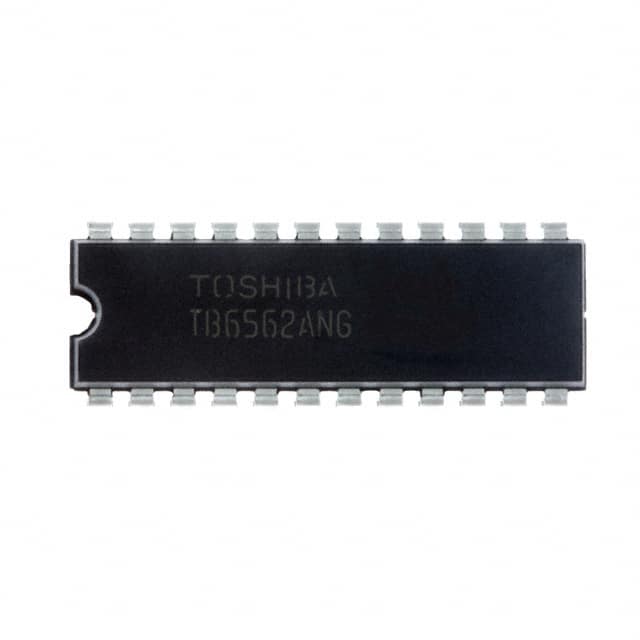
- Part No.:
- TB6561NG
- Manufacturer:
- Toshiba Semiconductor and Storage
- Category:
- Motor Drivers, Controllers
- Package:
- 24-SDIP (0.300", 7.62mm)
- Datasheet:
-
 TB6561NG.pdf
- Description:
- IC MOTOR DRIVER 10V-36V 24SDIP
- Quantity:
- Payment:

- Shipping:

Inventory:2,538
Please send an inquiry. Send us your inquiry, and we will respond immediately.
Product details
Overview
TB6561NG from Toshiba is a dual full-bridge driver IC for DC brush motors, integrating Bi-CMOS silicon monolithic technology with two independent H-bridge output stages. It delivers up to 1.5 A peak output current per channel, features 1.5 Ω typical total ON-resistance (upper + lower MOSFETs), and supports direct PWM current control with internal 500 ns dead-time generation for shoot-through prevention. It is used in bidirectional motor control applications such as robotic actuators and automated door systems.
For engineers reviewing the TB6561NG datasheet, TB6561NG pinout, TB6561NG application, or TB6561NG equivalent, key selection considerations include its 10–36 V operating supply range, thermal shutdown at 160°C (typ.), overcurrent protection at 2.5 A (typ.), and SDIP-24 package compatibility with through-hole PCB assembly and high-current motor drive layouts.
Technical Context
The TB6561NG implements two independent full-bridge output stages using low-RDS(on) N-channel MOSFETs, each controlled by dedicated logic inputs (IN1/IN2 per channel) and PWM direction pins (PWMA/PWMB). Its internal PWM current control system alternates between forward/reverse and short-brake modes without external timing components.
A shared thermal shutdown circuit (160°C activation, 40°C hysteresis) and per-channel overcurrent detection (2.5 A threshold, 10 μs glitch immunity) feed into a single CLD output pin. The IC also provides an internal 5 V regulator (Vreg) with ±2.5% tolerance at 1 mA load, decoupled via 0.1 μF capacitor to S-GND.
Key Specifications
| Parameter | Value and Actual Design Meaning |
|---|---|
| Output current (peak) | 1.5 A per channel - supports medium-power DC motors up to ~30 W at 24 V with appropriate heatsinking |
| Supply voltage (operating) | 10–36 V - compatible with standard 12 V/24 V industrial and automotive battery rails |
| ON-resistance (U+L) | 1.5 Ω (typ.) - minimizes conduction loss and heat generation during continuous drive |
| PWM frequency support | Up to 100 kHz - enables fine-grained motor speed resolution and reduced audible noise |
| Thermal shutdown threshold | 160°C (typ.) - protects die integrity during overload or poor thermal design; 40°C hysteresis prevents oscillation |
| Overcurrent limit | 2.5 A (typ.) - triggers automatic shutdown and recovery cycle to handle transient motor stalls |
| Vreg output | 5.0 V ±2.5% at 1 mA - powers external logic or sensors without auxiliary regulator |
Pinout & Package
Package: SDIP-24-P-300-1.78 - 24-pin single-in-line plastic package with 300 mil body width and 1.78 mm lead pitch, optimized for high-current through-hole mounting and thermal dissipation via P-GND pins.
| Pin/Terminal | Circuit Role | Design Meaning |
|---|---|---|
| 1, 12, 13, 24 | S-GND | Signal ground reference for logic inputs, Vreg, and CLD; must be star-connected to minimize noise coupling |
| 2 | Vreg | 5 V regulated output; requires 0.1 μF ceramic capacitor to S-GND for stability |
| 3 | SB | Standby enable: high = active, low = all outputs disabled (high-impedance); internal 100 kΩ pull-down |
| 4, 21 | PWMA / PWMB | Direction control inputs: 0/5 V logic toggles CW/CCW and short-brake modes; internal 100 kΩ pull-down |
| 5, 6, 19, 20 | IN1A / IN2A / IN1B / IN2B | Bridge state control inputs: define forward/reverse/stop/short-brake per channel; internal 100 kΩ pull-down |
| 7, 18, 23 | VCC | Motor power supply input (10–36 V); pins 7/18/23 must be externally shorted for balanced current sharing |
| 8, 11, 14, 17 | OUT1A / OUT2A / OUT2B / OUT1B | H-bridge output terminals; connect directly to motor coil ends; rated for 40 V max including back-EMF |
| 10, 15 | P-GNDA / P-GNDB | Power ground returns for chA/chB output stages; must be routed with low-inductance paths to minimize switching noise |
| 22 | CLD | Open-drain fault indicator: high = active overcurrent or thermal shutdown; supports automatic recovery |
Key Features
| Feature | Design Value |
|---|---|
| Internal dead-time generation | 500 ns (typ.) - eliminates need for external timing components and prevents shoot-through during PWM transitions |
| Direct PWM current control | Enables precise motor torque regulation without external current-sense amplifiers or feedback loops |
| Short-brake mode | Actively dissipates motor kinetic energy via simultaneous low-side FET conduction - faster stopping than coasting |
| Integrated 5 V regulator | Reduces BOM count by powering microcontroller I/O or level-shifting circuits from motor supply rail |
| Per-channel overcurrent detection | Monitors upper and lower transistors independently; triggers unified shutdown and auto-recovery sequence |
Applications
| Industrial Actuators | Automated Door Systems |
|---|---|
|
Use Scenario: Precise linear positioning of pneumatic or electric valve actuators in HVAC and process control cabinets. IC Role / Device Role / Timing Role: Dual H-bridge driver controlling two independent DC motors for push-pull motion and fail-safe braking. Use Value: Short-brake mode ensures rapid, repeatable stop position within ±0.5° mechanical tolerance without mechanical brakes. |
Use Scenario: Bidirectional control of sliding or swing doors in commercial buildings with obstacle detection and soft-start behavior. IC Role / Device Role / Timing Role: Motor interface translating microcontroller PWM and direction commands into full-bridge gate drive signals. Use Value: 1.5 A peak current and thermal shutdown prevent latch-up during jam detection, enabling safe reverse-on-stall behavior. |
| Robotic Joint Modules | Conveyor Belt Indexing |
|
Use Scenario: Compact elbow/wrist joint actuation in collaborative robots requiring reversible torque and position hold. IC Role / Device Role / Timing Role: Dual-channel bridge driver enabling independent control of two motors per joint for redundancy and torque vectoring. Use Value: Low 1.5 Ω RDS(on) minimizes self-heating during holding torque, extending joint lifetime in continuous-duty cycles. |
Use Scenario: Indexing conveyor segments in packaging lines where precise start/stop timing and load inertia management are critical. IC Role / Device Role / Timing Role: Motor driver executing synchronized acceleration/deceleration profiles via PWM duty-cycle modulation. Use Value: CLD pin integration allows PLC-level fault logging of overcurrent events without additional sensing hardware. |
Equivalent & Alternatives
The following parts are listed as comparable options for similar dual H-bridge motor driver applications.
| Alternative Part | Technical Difference | Application Difference | Selection Advice |
|---|---|---|---|
| STSPIN840 | 3-phase stepper driver with integrated current regulation; no short-brake mode; 1.8 A RMS per phase | Designed for open-loop stepper control, not brushed DC; lacks independent channel control logic | Choose STSPIN840 only if replacing stepper-based motion systems - not a functional substitute for TB6561NG's brushed DC bridge architecture |
| DRV8876N | Single H-bridge with 3.6 A peak current; integrated current sense amplifier; 4.5–37 V supply; QFN-16 package | Requires two units for dual-motor operation; no built-in short-brake or CLD fault reporting | Select DRV8876N when higher per-channel current and current monitoring are required, accepting doubled layout area and added control complexity |
Compared with STSPIN840 and DRV8876N, the TB6561NG uniquely integrates dual independent full-bridges, short-brake functionality, and unified fault reporting in a single SDIP-24 package - simplifying PCB layout and reducing firmware overhead for brushed DC motor systems requiring coordinated bidirectional control.
Availability
TB6561NG is available at Aetrix Electronics and suitable for industrial actuators, automated door systems, robotic joint modules, and conveyor belt indexing requiring stable component supply across multi-year production cycles.
Supply support for TB6561NG includes scheduled delivery planning, volume procurement assistance, BOM continuity management, traceable sourcing, and lifecycle availability coordination for OEM customers, industrial embedded developers, connected-device designers, and electronics production programs.
Manufacturer
Toshiba Electronic Devices & Storage Corporation designs and manufactures high-reliability semiconductor solutions for industrial, automotive, and consumer applications, with deep expertise in power management and motor control ICs.
The TB6561NG belongs to Toshiba's Bi-CMOS full-bridge driver product line, engineered specifically for cost-sensitive, medium-power brushed DC motor applications demanding robust protection, compact footprint, and simplified control interface.
FAQ
What is the maximum continuous output current rating for the TB6561NG?
The TB6561NG is rated for 1.5 A peak output current per channel under specified conditions (Ta = 25°C, with adequate heatsinking). Continuous current capability depends on ambient temperature, PCB copper area, and airflow; at 75°C ambient with 50 mm × 50 mm × 1.6 mm board (50% Cu), derating reduces usable current to approximately 0.8 A per channel to maintain junction temperature below 150°C. The TB6561NG datasheet specifies absolute maximum ratings and thermal resistance curves to guide real-world thermal design.
Does the TB6561NG support PWM speed control, and what is its maximum frequency?
Yes, the TB6561NG supports direct PWM speed control via its PWMA and PWMB pins, which accept 0–5 V logic-level signals. It operates reliably up to 100 kHz PWM frequency, enabling smooth motor velocity regulation and reduced acoustic noise. Internal dead-time generation (500 ns typ.) ensures safe switching transitions without external timing components. The TB6561NG PWM input circuitry includes hysteresis (0.4 V typ.) to reject noise and ensure clean edge detection.
How does the CLD pin function on the TB6561NG, and what fault conditions trigger it?
The CLD pin on the TB6561NG is an open-drain output that goes high during overcurrent detection (ILIM = 2.5 A typ.) in either channel or thermal shutdown (TSD = 160°C typ.). It remains high until the fault condition clears - current drops below threshold or junction temperature falls below 120°C (40°C hysteresis). The TB6561NG CLD circuit supports automatic recovery and requires an external pull-up resistor (typically 10 kΩ to 5 V) for proper logic-level signaling to host controllers.
What are the recommended decoupling capacitors for the TB6561NG power and logic supplies?
For the TB6561NG, place a 0.1 μF ceramic capacitor between Vreg (pin 2) and S-GND (pins 1/12/13/24) to stabilize the internal 5 V regulator. For motor supply filtering, use ≥100 μF low-ESR electrolytic capacitor between VCC (pins 7/18/23) and P-GNDA/P-GNDB (pins 10/15), located as close as possible to the IC. Additional 0.01 μF ceramic capacitors may be added in parallel for high-frequency noise suppression. These values are specified in the TB6561NG application circuit and thermal derating guidelines.
Can the TB6561NG drive two separate DC motors simultaneously, and how are their control signals isolated?
Yes, the TB6561NG integrates two fully independent full-bridge drivers (chA and chB), each with dedicated input pins (IN1A/IN2A/PWMA and IN1B/IN2B/PWMB), output terminals (OUT1A/OUT2A and OUT1B/OUT2B), and power grounds (P-GNDA/P-GNDB). Control signals are electrically isolated at the logic level - no shared control path exists between channels. The TB6561NG allows asynchronous operation: one motor can run forward while the other executes short-brake, enabling complex motion sequences in dual-motor systems.
TB6561NG Specifications
- Product attributes
- Attribute value
- Manufacturer:
- Toshiba Semiconductor and Storage
- Series:
- -
- Package/Case:
- 24-SDIP (0.300", 7.62mm)
- Packaging:
- Tube
- Product Status:
- Obsolete
- Motor Type - Stepper:
- -
- Motor Type - AC, DC:
- Brushed DC
- Function:
- Driver - Fully Integrated, Control and Power Stage
- Output Configuration:
- Half Bridge (4)
- Interface:
- PWM
- Technology:
- Bi-CMOS
- Step Resolution:
- -
- Applications:
- General Purpose
- Current - Output:
- 1.5A
- Voltage - Supply:
- 10V ~ 36V
- Voltage - Load:
- 10V ~ 36V
- Operating Temperature:
- -20°C ~ 85°C (TA)
- Grade:
- -
- Qualification:
- -
- Mounting Type:
- Through Hole
- Supplier Device Package:
- 24-SDIP
TB6561NG FAQ
1.How can I place an order for TB6561NG through Aetrix?
Please submit a Request for Quotation (RFQ) for TB6561NG on Aetrix. Our sales agent will provide a competitive quotation and guide you through the order confirmation once you accept the terms.
2.Are the price and stock information for TB6561NG reliable?
The price and inventory of TB6561NG are updated periodically and may fluctuate due to market conditions. Stock and pricing data are typically refreshed every 24 hours. Quotation validity for TB6561NG is usually 5 days.
3.What payment methods are accepted for TB6561NG?
We accept Wire Transfer, PayPal, Credit Card, Western Union, MoneyGram, and Escrow for TB6561NG transactions.
Note: Certain payment methods may incur a processing fee.
4.How is shipping managed for TB6561NG?
TB6561NG orders can be shipped via leading logistics carriers, including DHL, UPS, FedEx, TNT, or Registered Mail.
Once your TB6561NG order is processed, you will receive an email with the shipment details and tracking number.
Note: Tracking information may take up to 24 hours to appear. Express delivery typically takes 3–5 business days.
5.How can I obtain technical support or documentation for TB6561NG?
For technical support, including TB6561NG datasheets, pinout diagrams, or application guidance, please contact our engineering support team. They can provide detailed documentation and assistance for your TB6561NG requirements.
6.How does Aetrix verify that TB6561NG is sourced from the original manufacturer or authorized distributors?
All TB6561NG products on Aetrix are procured from qualified distributors and authorized channels. Our dedicated quality assurance team conducts strict verification, including traceability checks and, if necessary, third-party testing. This ensures that TB6561NG meets industry standards.
7.What is the process for return or replacement of TB6561NG?
All TB6561NG units undergo pre-shipment inspection (PSI). If there is an issue with TB6561NG, returns or replacements are accepted under the following conditions:
1.Quantity discrepancies, incorrect items, or visible external defects (such as breakage or corrosion), acknowledged by Aetrix.
2.The issue is reported within 90 days of delivery.
3.The TB6561NG part is unused and in its original packaging.
Return procedure for TB6561NG:
1.Submit a request within 90 days.
2.Obtain a Return Material Authorization (RMA) from Aetrix.
TB6561NG Tags

-
DRV2603RUNR
Texas Instruments

-
DRV8837CDSGR
Texas Instruments

-
DRV8837DSGR
Texas Instruments
-
DRV8838DSGR
Texas Instruments

-
DRV8839DSSR
Texas Instruments

-
EMC2301-1-ACZL-TR
Microchip Technology
-
DRV8231ADSGR
Texas Instruments

-
EMC2302-2-AIZL-TR
Microchip Technology

-
DRV8800PWPR
Texas Instruments
-
DRV8835DSSR
Texas Instruments

-
EMC2303-1-KP-TR
Microchip Technology

-
DRV8876PWPR
Texas Instruments
Tech Hub

Counterfeit components can hide behind convincing markings and passing basic function tests. This engineering reference covers source traceability, external inspection, X-ray, XRF, electrical testing, …

A practical engineering and sourcing framework covering lifecycle verification, lifetime-buy calculations, replacement qualification, supplier checks and counterfeit-risk controls.

TTL and CMOS logic families differ in thresholds, loading, output drive, power and timing. This engineering guide compares 74HC and 74HCT, calculates noise margins and checks 3.3 V/5 V compatibility.

A practical engineering guide to 3.3V and 5V logic compatibility, input thresholds, resistor dividers, translator ICs, MOSFET level shifting, I2C pull-ups, timing limits and power-sequencing risks.

The 74HC595 uses push-pull logic outputs, while the TPIC6B595 uses 50 V open-drain DMOS sinks for higher-power loads. This guide compares timing, current limits, 3.3 V interfacing, load wiring, thermal…

The 74HC595 converts serial data into eight stable parallel outputs. This guide covers pin functions, shift and storage timing, OE and MR behavior, drive-current limits, cascading, voltage compatibilit…

A technical comparison of level-sensitive latches and edge-triggered flip-flops, covering timing windows, setup and hold limits, master–slave operation, time borrowing, race-through, HDL inference and…

A D latch stores one bit while Enable controls when data can pass. This reference covers gate-level operation, truth tables, transparency, setup and hold timing, LE versus OE, common ICs and practical …

An SR latch stores one bit through cross-coupled feedback. This engineering reference covers NOR and NAND implementations, truth tables, forbidden-state recovery, gated operation, switch debouncing, fa…

Latch circuits retain one bit through feedback. This technical reference covers SR and D latches, truth tables, transparency, timing limits, latch-versus-flip-flop behavior, applications and common log…


