
 My Inquiry
 My Account


Toshiba Semiconductor and Storage TB6561NG,8
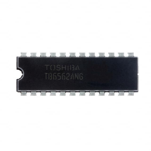
- Part No.:
- TB6561NG,8
- Manufacturer:
- Toshiba Semiconductor and Storage
- Category:
- Motor Drivers, Controllers
- Package:
- 24-SDIP (0.300", 7.62mm)
- Datasheet:
-
 TB6561NG,8.pdf
- Description:
- IC MOTOR DRIVER 10V-36V 24SDIP
- Quantity:
- Payment:

- Shipping:

Inventory:3,934
Please send an inquiry. Send us your inquiry, and we will respond immediately.
Product details
Overview
TB6561NG from Toshiba is a dual full-bridge DC motor driver IC integrating Bi-CMOS silicon monolithic technology, delivering 1.5 A peak output current per channel with 1.5 Ω typical ON-resistance (upper + lower transistors), 40 V absolute max supply voltage, and integrated PWM current control for brushed DC motor control in compact industrial actuators.
For engineers reviewing the TB6561NG datasheet, TB6561NG pinout, TB6561NG application, or TB6561NG equivalent, this page provides verified functional roles, thermal shutdown behavior at 160°C, CLD fault signaling, and direct PWM interface timing - all critical for motor control loop design, PCB layout validation, and overcurrent protection integration.
Technical Context
The TB6561NG implements two independent H-bridge channels (A and B), each with complementary MOSFET output stages controlled by IN1/IN2 logic inputs and PWM-modulated direction signals (PWMA/PWMB). It uses internal dead-time generation (500 ns typ.) to prevent shoot-through during switching transitions.
Its protection architecture includes per-channel overcurrent detection (2.5 A typ. threshold, 10 μs minimum pulse width), shared thermal shutdown (160°C activation, 40°C hysteresis), and CLD pin reporting of both fault conditions with automatic recovery - all operating within 10–36 V motor supply range and 5 V logic interface compliance.
Key Specifications
| Parameter | Value and Actual Design Meaning |
|---|---|
| Max Output Current | 1.5 A peak per channel - supports small-to-medium brushed DC motors up to ~30 W at 24 V |
| ON-Resistance (U+L) | 1.5 Ω typ. - enables >85% efficiency at 1 A load with minimal thermal rise on SDIP-24 package |
| Supply Voltage Range | 10–36 V operating / 40 V absolute max - compatible with 12 V and 24 V industrial power rails including back-EMF margin |
| PWM Frequency Support | Up to 100 kHz - allows fine-grained speed resolution and low audible noise in motor drive applications |
| Thermal Shutdown | 160°C activation with 40°C hysteresis - prevents permanent damage during sustained overload or poor heatsinking |
| Current Limit Threshold | 2.5 A typ. (1.5–3.5 A range) - triggers automatic 50 μs off-cycle to clear transient overloads without MCU intervention |
| Vreg Output | 5.0 V ±2.5% at 1 mA - powers external logic or sensors; requires 0.1 μF decoupling to S-GND |
Pinout & Package
Package: SDIP-24-P-300-1.78 (24-pin shrink dual in-line plastic, 300 mil width, 1.78 mm thickness, 1.62 g typical weight).
| Pin/Terminal | Circuit Role | Design Meaning |
|---|---|---|
| 1, 12, 13, 24 | S-GND | Signal ground reference for logic inputs, Vreg, and CLD - must be star-connected to minimize noise coupling |
| 2 | Vreg | 5 V regulated output - supplies external circuitry; requires local 0.1 μF capacitor to S-GND |
| 3 | SB | Standby enable - high = active, low = all outputs disabled with 1.5–3 mA standby current |
| 4, 21 | PWMA / PWMB | Direction control inputs - accept 0/5 V PWM for speed regulation; internal 100 kΩ pull-down |
| 5, 6, 19, 20 | IN1A/IN2A/IN1B/IN2B | H-bridge state control - define CW/CCW/short-brake/stop modes; internal 100 kΩ pull-down |
| 7, 18, 23 | VCC | Motor power input - three pins must be shorted externally; supports 10–36 V with 40 V abs max |
| 8, 11, 17, 14 | OUT1A/OUT2A/OUT1B/OUT2B | H-bridge outputs - connect directly to motor coil terminals; rated for 40 V and 1.5 A peak |
| 10, 15 | P-GNDA / P-GNDB | Power ground returns - separate from signal ground to avoid ground bounce in high-current paths |
| 22 | CLD | Fault indicator - open-drain output pulled high during overcurrent or thermal shutdown; auto-recovers |
Key Features
| Feature | Design Value |
|---|---|
| Integrated PWM current control | Enables closed-loop speed regulation without external current-sense amplifiers or DACs |
| Internal 500 ns dead-time generation | Eliminates need for external timing components and prevents shoot-through in both CW/CCW and brake transitions |
| Dual independent H-bridge channels | Allows simultaneous bidirectional control of two DC motors or coordinated motion of one 2-phase motor |
| CLD fault reporting with auto-recovery | Reduces firmware complexity by providing single-pin status indication and self-clearing fault handling |
| Low 1.5 Ω total ON-resistance | Lowers conduction losses and junction temperature rise, enabling higher continuous current in constrained thermal environments |
Applications
| Industrial Actuators | Automated Valves |
|---|---|
Use Scenario: Precise linear positioning of pneumatic or hydraulic valve stems using 24 V brushed DC motors in factory automation panels. IC Role / Device Role / Timing Role: Dual H-bridge driver executing forward/reverse/short-brake commands from PLC I/O, with PWM speed modulation synchronized to process timing cycles. Use Value: Eliminates external gate drivers and current-sense circuits while maintaining <100 ms response time and thermal resilience in enclosed cabinets. | Use Scenario: Remote-controlled HVAC damper actuation in commercial building management systems with 12 V DC supply constraints. IC Role / Device Role / Timing Role: Motor driver interpreting Modbus RTU command packets via microcontroller GPIO, managing stall detection and safe shutdown on position limit hit. Use Value: CLD pin integration simplifies fault logging; 10–36 V operating range accommodates brownout conditions without reset. |
| Medical Pump Modules | Robotic Joint Controllers |
Use Scenario: Peristaltic fluid delivery in portable infusion pumps requiring silent, low-ripple motor operation and battery-efficient current limiting. IC Role / Device Role / Timing Role: Dual-channel driver powering two synchronized pump heads with independent PWM duty cycle control for flow rate calibration. Use Value: 100 kHz PWM support enables ultrasonic switching frequency to eliminate audible whine; thermal shutdown prevents overheating during occlusion events. | Use Scenario: Low-inertia joint actuation in collaborative robots where rapid direction reversal and dynamic braking are required for safety compliance. IC Role / Device Role / Timing Role: Real-time motor driver executing torque/position commands from motion controller, using short-brake mode for emergency stop with <5 ms decay time. Use Value: Internal dead-time ensures robust commutation during 10 kHz direction toggling; P-GND separation minimizes encoder signal corruption. |
Equivalent & Alternatives
The following parts are listed as comparable options for similar dual H-bridge motor driver applications.
| Alternative Part | Technical Difference | Application Difference | Selection Advice |
|---|---|---|---|
| TB6612FNG | Lower RDS(on) (0.66 Ω typ.), higher 3.2 A peak current, smaller SSOP-24 package, no Vreg output | Better suited for higher-power 24 V motors; lacks onboard 5 V regulator for auxiliary logic | Select when thermal budget is tighter and external 5 V rail is available |
| DRV8876N | Integrated current sense amplifier, SPI register interface, 3.6 A peak, thermally enhanced HTSSOP-28 | Enables closed-loop current control and diagnostics via digital interface; requires SPI host firmware | Select when precise current monitoring or programmable protection thresholds are required |
Compared with TB6612FNG and DRV8876N, the TB6561NG offers unique value in cost-sensitive industrial designs needing integrated 5 V regulation, simple GPIO control, and proven reliability in long-lifecycle embedded systems - without demanding advanced communication or ultra-low RDS(on).
Availability
TB6561NG is available at Aetrix Electronics and suitable for industrial actuators, automated valves, medical pump modules, robotic joint controllers, and HVAC damper systems requiring stable component supply across multi-year production programs.
Supply support for TB6561NG includes scheduled delivery planning, volume procurement assistance, BOM continuity management, traceable sourcing, and lifecycle availability coordination for OEM customers, industrial embedded developers, connected-device designers, and electronics production programs.
Manufacturer
Toshiba Electronic Devices & Storage Corporation designs and manufactures high-reliability semiconductor solutions for industrial, automotive, and consumer applications, with deep expertise in power management and motor control ICs.
The TB6561NG belongs to Toshiba's Bi-CMOS motor driver product line, engineered specifically for cost-effective, thermally robust dual H-bridge control of brushed DC motors in space-constrained industrial equipment.
FAQ
What is the maximum continuous output current rating for TB6561NG?
The TB6561NG is rated for 1.5 A peak output current per channel under specified thermal conditions. Continuous current depends on PCB copper area, ambient temperature, and heatsinking - with 2.5 W max power dissipation on a 50 mm × 50 mm × 1.6 mm board (50% Cu). At 25°C ambient and proper layout, TB6561NG supports ~1.0 A continuous per channel without exceeding 150°C junction temperature. Always verify thermal performance in final system configuration.
How does the CLD pin function on TB6561NG?
The CLD pin on TB6561NG is an open-drain fault indicator that goes high during overcurrent detection (2.5 A typ.) or thermal shutdown (160°C). It automatically returns low once the fault condition clears - e.g., current drops below threshold or junction cools below 120°C. The TB6561NG CLD pin requires an external pull-up resistor (typically 10 kΩ to 5 V) and supports direct connection to MCU interrupt inputs for real-time fault response without polling.
Can TB6561NG drive two independent motors simultaneously?
Yes, TB6561NG integrates two fully independent full-bridge channels (A and B), each with dedicated IN1/IN2 control inputs, PWM direction pins (PWMA/PWMB), and output pairs (OUT1A/OUT2A and OUT1B/OUT2B). This allows simultaneous bidirectional control of two brushed DC motors - for example, left/right wheel drives in differential-drive robots or dual-axis positioning stages - with no shared timing or current limitations between channels.
What is the purpose of the Vreg pin on TB6561NG?
The Vreg pin on TB6561NG delivers a regulated 5.0 V ±2.5% output at up to 1 mA, intended to power external logic such as microcontroller GPIOs, level shifters, or sensor interfaces. It must be decoupled with a 0.1 μF ceramic capacitor to S-GND, placed as close as possible to the pin. This eliminates the need for a separate LDO in space-constrained designs - a key differentiator of the TB6561NG versus many competing dual H-bridge drivers.
Does TB6561NG require external dead-time circuitry for PWM operation?
No, TB6561NG incorporates internal dead-time generation of 500 ns (typ.) between upper and lower transistor switching transitions. This prevents shoot-through current in both direction changes (CW ↔ CCW) and mode transitions (e.g., CW ↔ short-brake), eliminating the need for external timing components or complex gate-drive sequencing. The TB6561NG achieves synchronous rectification and high efficiency without external dead-time management.
TB6561NG,8 Specifications
- Product attributes
- Attribute value
- Manufacturer:
- Toshiba Semiconductor and Storage
- Series:
- -
- Package/Case:
- 24-SDIP (0.300", 7.62mm)
- Packaging:
- Tray
- Product Status:
- Active
- Motor Type - Stepper:
- -
- Motor Type - AC, DC:
- Brushed DC
- Function:
- Driver - Fully Integrated, Control and Power Stage
- Output Configuration:
- Half Bridge (4)
- Interface:
- PWM
- Technology:
- Bi-CMOS
- Step Resolution:
- -
- Applications:
- General Purpose
- Current - Output:
- 1.5A
- Voltage - Supply:
- 10V ~ 36V
- Voltage - Load:
- 10V ~ 36V
- Operating Temperature:
- -20°C ~ 85°C (TA)
- Grade:
- -
- Qualification:
- -
- Mounting Type:
- Through Hole
- Supplier Device Package:
- 24-SDIP
TB6561NG,8 FAQ
1.How can I place an order for TB6561NG,8 through Aetrix?
Please submit a Request for Quotation (RFQ) for TB6561NG,8 on Aetrix. Our sales agent will provide a competitive quotation and guide you through the order confirmation once you accept the terms.
2.Are the price and stock information for TB6561NG,8 reliable?
The price and inventory of TB6561NG,8 are updated periodically and may fluctuate due to market conditions. Stock and pricing data are typically refreshed every 24 hours. Quotation validity for TB6561NG,8 is usually 5 days.
3.What payment methods are accepted for TB6561NG,8?
We accept Wire Transfer, PayPal, Credit Card, Western Union, MoneyGram, and Escrow for TB6561NG,8 transactions.
Note: Certain payment methods may incur a processing fee.
4.How is shipping managed for TB6561NG,8?
TB6561NG,8 orders can be shipped via leading logistics carriers, including DHL, UPS, FedEx, TNT, or Registered Mail.
Once your TB6561NG,8 order is processed, you will receive an email with the shipment details and tracking number.
Note: Tracking information may take up to 24 hours to appear. Express delivery typically takes 3–5 business days.
5.How can I obtain technical support or documentation for TB6561NG,8?
For technical support, including TB6561NG,8 datasheets, pinout diagrams, or application guidance, please contact our engineering support team. They can provide detailed documentation and assistance for your TB6561NG,8 requirements.
6.How does Aetrix verify that TB6561NG,8 is sourced from the original manufacturer or authorized distributors?
All TB6561NG,8 products on Aetrix are procured from qualified distributors and authorized channels. Our dedicated quality assurance team conducts strict verification, including traceability checks and, if necessary, third-party testing. This ensures that TB6561NG,8 meets industry standards.
7.What is the process for return or replacement of TB6561NG,8?
All TB6561NG,8 units undergo pre-shipment inspection (PSI). If there is an issue with TB6561NG,8, returns or replacements are accepted under the following conditions:
1.Quantity discrepancies, incorrect items, or visible external defects (such as breakage or corrosion), acknowledged by Aetrix.
2.The issue is reported within 90 days of delivery.
3.The TB6561NG,8 part is unused and in its original packaging.
Return procedure for TB6561NG,8:
1.Submit a request within 90 days.
2.Obtain a Return Material Authorization (RMA) from Aetrix.
TB6561NG,8 Tags

-
DRV2603RUNR
Texas Instruments

-
DRV8837CDSGR
Texas Instruments

-
DRV8837DSGR
Texas Instruments
-
DRV8838DSGR
Texas Instruments

-
DRV8839DSSR
Texas Instruments

-
EMC2301-1-ACZL-TR
Microchip Technology
-
DRV8231ADSGR
Texas Instruments

-
EMC2302-2-AIZL-TR
Microchip Technology

-
DRV8800PWPR
Texas Instruments
-
DRV8835DSSR
Texas Instruments

-
EMC2303-1-KP-TR
Microchip Technology

-
DRV8876PWPR
Texas Instruments
Tech Hub

Counterfeit components can hide behind convincing markings and passing basic function tests. This engineering reference covers source traceability, external inspection, X-ray, XRF, electrical testing, …

A practical engineering and sourcing framework covering lifecycle verification, lifetime-buy calculations, replacement qualification, supplier checks and counterfeit-risk controls.

TTL and CMOS logic families differ in thresholds, loading, output drive, power and timing. This engineering guide compares 74HC and 74HCT, calculates noise margins and checks 3.3 V/5 V compatibility.

A practical engineering guide to 3.3V and 5V logic compatibility, input thresholds, resistor dividers, translator ICs, MOSFET level shifting, I2C pull-ups, timing limits and power-sequencing risks.

The 74HC595 uses push-pull logic outputs, while the TPIC6B595 uses 50 V open-drain DMOS sinks for higher-power loads. This guide compares timing, current limits, 3.3 V interfacing, load wiring, thermal…

The 74HC595 converts serial data into eight stable parallel outputs. This guide covers pin functions, shift and storage timing, OE and MR behavior, drive-current limits, cascading, voltage compatibilit…

A technical comparison of level-sensitive latches and edge-triggered flip-flops, covering timing windows, setup and hold limits, master–slave operation, time borrowing, race-through, HDL inference and…

A D latch stores one bit while Enable controls when data can pass. This reference covers gate-level operation, truth tables, transparency, setup and hold timing, LE versus OE, common ICs and practical …

An SR latch stores one bit through cross-coupled feedback. This engineering reference covers NOR and NAND implementations, truth tables, forbidden-state recovery, gated operation, switch debouncing, fa…

Latch circuits retain one bit through feedback. This technical reference covers SR and D latches, truth tables, transparency, timing limits, latch-versus-flip-flop behavior, applications and common log…


