
 My Inquiry
 My Account


Toshiba Semiconductor and Storage TB6634FNG,C,8,EL
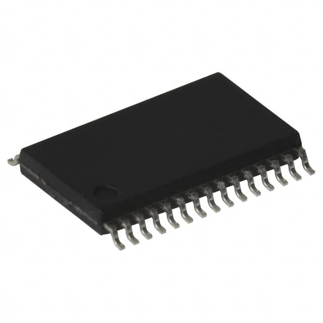
- Part No.:
- TB6634FNG,C,8,EL
- Manufacturer:
- Toshiba Semiconductor and Storage
- Category:
- Motor Drivers, Controllers
- Package:
- 30-LSSOP (0.220", 5.60mm Width)
- Datasheet:
-
 TB6634FNG,C,8,EL.pdf
- Description:
- IC MOTOR DRVR 6.5V-16.5V 30SSOP
- Quantity:
- Payment:

- Shipping:

Inventory:1,862
Please send an inquiry. Send us your inquiry, and we will respond immediately.
Product details
Overview
TB6634FNG,C,8,EL from Toshiba Electronic Devices & Storage Corporation is a 3-phase full-wave sine-wave PWM brushless motor controller IC designed for motor fan applications. It delivers sine-wave commutation (180°) above 1 Hz, square-wave (120°) at startup, supports 0°–58° lead angle control in 32 steps, operates from 6 V to 16.5 V supply, and integrates a 5 V/30 mA voltage regulator.
For engineers reviewing the TB6634FNG,C,8,EL datasheet, TB6634FNG,C,8,EL pinout, TB6634FNG,C,8,EL application, or TB6634FNG,C,8,EL equivalent, key selection considerations include its Hall-sensor-based position estimation, programmable dead time (~2.0 μs at 4.5 MHz), carrier frequency derivation (fOSC/252), motor restrained detection via TR pin, and dual-mode drive switching based on VSP voltage and Hall frequency.
Technical Context
The TB6634FNG,C,8,EL implements sensor-based BLDC control using three Hall inputs (HUP/HUM, HVP/HVM, HWP/HWM) to estimate rotor position and generate modulated sine-wave PWM outputs. Its internal 6-bit triangular wave generator sets the carrier frequency at fOSC/252, while a 5-bit ADC digitizes LPF/LA voltage to select lead angle in 32 discrete steps (0°–58°).
It features dual commutation modes: square-wave (120°) below 1 Hz for reliable startup, and sine-wave (180°) above 1 Hz for low-noise, high-efficiency operation. Protection logic includes current-limiting via Idc pin (0.3 V threshold), Vdc-based overvoltage detection (4.1 V trip), RES-driven abnormal shutdown, and motor restrained detection with configurable timing via external TR capacitor.
Key Specifications
| Parameter | Value and Actual Design Meaning |
|---|---|
| Supply Voltage Range | VCC = 6 V to 16.5 V - powers internal logic, gate drivers, and 5 V regulator; absolute max 18 V |
| Lead Angle Control | 0° to 58° in 32 steps - set by 0–5 V analog input on LPF/LA pin; enables torque optimization across speed/load |
| Carrier Frequency | fOSC/252 - derived from CR oscillator (3–6 MHz); yields ~18–23 kHz PWM for smooth motor control |
| Dead Time | ~2.0 μs at fOSC = 4.5 MHz - digitally inserted between high-side and low-side switching to prevent shoot-through |
| Vrefout | 5.0 V ±0.5 V / 30 mA max - stable reference for external circuitry and internal ADCs; requires local decoupling cap |
| Motor Restraint Detection | Configurable via TR pin capacitor - enables 1:6 run/stop cycling when Hall signal stalls below 1 Hz (CW) or 5 Hz (CCW) |
| Current Limit Threshold | 0.3 V (typ.) on Idc pin - disables outputs after one carrier cycle when DC-link current exceeds limit |
| FG Output Resolution | Selectable 1 or 3 pulses per electrical revolution - controlled by FGC pin; supports precise speed feedback |
Pinout & Package
Package: SOP30 (30-pin small outline package), body size 12.8 mm × 7.6 mm × 2.45 mm, pitch 1.27 mm, RoHS-compliant.
| Pin/Terminal | Circuit Role | Design Meaning |
|---|---|---|
| U, V, W | High-side commutation outputs | Push-pull, Vrefout-referenced; drive external high-side N-channel MOSFET gates in 3-phase bridge |
| X, Y, Z | Low-side commutation outputs | Push-pull, Vrefout-referenced; drive external low-side N-channel MOSFET gates; include 8% refresh duty |
| HUP, HUM, HVP, HVM, HWP, HWM | Hall position sensor inputs | Differential digital inputs with internal pull-ups and digital filtering; detect rotor position for 120°/180° commutation |
| LPF/LA | Lead angle analog control input | RC low-pass filtered input (100 kΩ on-chip); 0–5 V maps linearly to 0°–58° lead angle in 32 steps |
| VSP | Voltage command input | Analog speed command (0–10 V); determines conduction duty (up to 92%), mode transition (square→sine at ~7.9 V), and refresh behavior |
| Idc | Current limit monitor input | Accepts DC-link shunt voltage; trips output disable when >0.3 V (typ.); includes analog + digital filtering |
| RES | Abnormal detection enable | Active-high logic input; forces all outputs low when low; internal pull-down; used for external fault signaling |
| TR | Motor restraint detection | Capacitor-connected input; configures stall detection timeout (e.g., 0.01 μF → ~4.8 s run / ~28.6 s stop) |
| Vdc | Motor supply voltage monitor | 2-bit ADC input; triggers lead angle correction (±1.875°–5.625°) or shutdown (≥4.1 V) based on hysteresis thresholds |
| FGC | FG resolution select | Active-low digital input; selects 1 ppr (L) or 3 ppr (H/open) FG output for speed monitoring |
| CW/CCW | Rotation direction control | Active-high logic input; L = clockwise, H = counterclockwise; also inverts Hall interpretation for reverse rotation detection |
| Vrefout | Internal reference voltage output | 5.0 V ±0.5 V regulated output; supplies external circuits and internal references; max 30 mA load |
| GND, VCC | Power supply terminals | VCC accepts 6–16.5 V; GND is common return for analog/digital/power domains; thermal pad connected to GND |
Key Features
| Feature | Design Value |
|---|---|
| Sine-wave PWM commutation | Enables low-acoustic-noise, high-efficiency motor operation above 1 Hz; reduces torque ripple vs. square-wave |
| Programmable lead angle (0°–58°) | Compensates for back-EMF phase lag across speed range; improves efficiency and stability under varying load |
| Integrated 5 V/30 mA voltage regulator | Eliminates need for external LDO; powers Hall sensors, microcontrollers, or level-shifting circuitry directly |
| Dual commutation mode auto-switching | Starts in robust 120° square-wave mode ≤1 Hz; transitions seamlessly to optimized 180° sine-wave mode >1 Hz |
| Hall-input-based position estimation | Uses edge timing of U/V/W Hall signals to reconstruct rotor position without external encoder or resolver |
| Comprehensive protection suite | Includes overcurrent (Idc), overvoltage (Vdc), abnormal position (UVW=000/111), undervoltage lockout (VCC), and motor stall (TR) |
Applications
| CPU Cooler Fan | Server Chassis Fan |
|---|---|
Use Scenario: High-reliability, variable-speed cooling in air-cooled server CPUs where acoustic noise and power efficiency are critical. IC Role / Device Role / Timing Role: Primary BLDC motor controller managing commutation, lead angle, and speed regulation via VSP analog input and Hall feedback. Use Value: Sine-wave drive reduces audible whine; programmable lead angle maintains torque at low speeds; integrated Vrefout simplifies system BOM. | Use Scenario: Multi-fan thermal management in 1U/2U rack servers requiring coordinated speed control and fault reporting. IC Role / Device Role / Timing Role: Centralized motor controller per fan, using FG output (1/3 ppr selectable) for closed-loop RPM feedback and RES pin for system-level fault propagation. Use Value: Motor restrained detection prevents thermal runaway during fan blockage; Vdc monitoring enables supply health awareness. |
| Network Switch Fan | Industrial Enclosure Fan |
Use Scenario: Compact, high-airflow cooling in space-constrained network switches operating continuously at elevated ambient temperatures. IC Role / Device Role / Timing Role: Standalone motor driver handling startup, direction (CW/CCW), and dynamic lead angle adjustment based on temperature-compensated VSP command. Use Value: SOP30 package enables dense PCB layout; wide 6–16.5 V VCC range accommodates varied DC input rails (12 V nominal, ±10% tolerance). | Use Scenario: Harsh-environment ventilation in industrial control cabinets exposed to dust, vibration, and wide temperature swings (−30°C to +115°C). IC Role / Device Role / Timing Role: Robust BLDC controller with extended temperature rating, RES-driven emergency shutdown, and TR-based stall recovery for unattended operation. Use Value: Built-in digital filtering on Hall inputs rejects EMI; hysteresis on Vdc/RES pins prevents chatter-induced false trips. |
Equivalent & Alternatives
The following parts are listed as comparable options for similar 3-phase BLDC motor controller applications.
| Alternative Part | Technical Difference | Application Difference | Selection Advice |
|---|---|---|---|
| STSPIN32F0A | Integrated 32-bit ARM Cortex-M0 MCU + gate drivers; requires firmware development; no native sine-wave PWM generator | Best for systems needing field-oriented control (FOC), custom diagnostics, or multi-motor coordination | Choose STSPIN32F0A if firmware flexibility and advanced control algorithms outweigh the benefit of TB6634FNG,C,8,EL's plug-and-play sine-wave generation. |
| MP6532 | External oscillator required; fixed 30° max lead angle; no motor restraint detection or Vdc monitoring | Suitable for cost-sensitive, lower-performance fans where basic 120° commutation suffices | Choose MP6532 only when simplified feature set and lower BOM cost are prioritized over TB6634FNG,C,8,EL's adaptive lead angle and comprehensive protection. |
Compared with STSPIN32F0A and MP6532, the TB6634FNG,C,8,EL provides out-of-the-box sine-wave PWM with hardware-programmable lead angle and integrated motor protection functions-reducing firmware burden and improving reliability in fan-specific applications without requiring external microcontroller support or sacrificing diagnostic capability.
Availability
TB6634FNG,C,8,EL is available at Aetrix Electronics and suitable for CPU cooler fan, server chassis fan, and network switch fan applications requiring stable component supply, long-term industrial lifecycle support, and RoHS-compliant packaging.
Supply support for TB6634FNG,C,8,EL includes scheduled delivery planning, volume procurement assistance, BOM continuity management, traceable sourcing, and lifecycle availability coordination for OEM customers, industrial embedded developers, connected-device designers, and electronics production programs.
Manufacturer
Toshiba Electronic Devices & Storage Corporation designs and manufactures power semiconductors, motor drivers, and logic ICs for industrial, automotive, and consumer applications.
The TB6634FNG,C,8,EL belongs to Toshiba's dedicated BLDC motor controller product line, engineered specifically for low-noise, high-efficiency fan motor control in computing and communications infrastructure.
FAQ
What is the function of the LPF/LA pin on the TB6634FNG,C,8,EL?
The LPF/LA pin on the TB6634FNG,C,8,EL is an analog input that sets the motor lead angle from 0° to 58° in 32 discrete steps. A voltage between 0 V and 5.0 V applied to this pin-filtered through an external capacitor and the device's internal 100 kΩ resistor-directly determines the commutation advance. For example, 2.5 V yields approximately 30° lead angle. This function compensates for back-EMF phase lag, optimizing torque and efficiency across the motor's speed range. The TB6634FNG,C,8,EL uses this setting exclusively in sine-wave PWM mode.
How does the TB6634FNG,C,8,EL switch between square-wave and sine-wave commutation modes?
The TB6634FNG,C,8,EL automatically switches commutation modes based on Hall sensor frequency and VSP voltage. Below 1 Hz Hall input frequency (at fOSC = 4.5 MHz), it uses 120° square-wave drive for reliable startup. Above 1 Hz, it transitions to 180° sine-wave PWM drive. The transition point is also influenced by VSP: sine-wave mode activates when VSP exceeds ~7.9 V (typical), regardless of Hall frequency. The TB6634FNG,C,8,EL performs this switching autonomously using internal position estimation and modulation logic-no external intervention is required.
What protection features are implemented in the TB6634FNG,C,8,EL?
The TB6634FNG,C,8,EL integrates six core protection mechanisms: (1) Overcurrent detection via Idc pin (0.3 V threshold), (2) Motor supply overvoltage detection via Vdc pin (4.1 V trip), (3) Abnormal Hall input detection (UVW = 000 or 111), (4) Undervoltage lockout on VCC (4.0 V turn-off), (5) Motor restrained detection via TR pin with user-configurable timing, and (6) RES pin–driven emergency shutdown. All protections force commutation outputs low and are designed to prevent damage to external power devices. Each has defined hysteresis and digital filtering to avoid false triggering, ensuring robust operation in noisy environments.
Can the TB6634FNG,C,8,EL drive motors directly, or does it require external power devices?
The TB6634FNG,C,8,EL is a gate driver controller IC and cannot drive motors directly. It provides six push-pull commutation outputs (U, V, W, X, Y, Z) referenced to Vrefout (5 V), each capable of ±2 mA sink/source. These signals are intended to drive the gates of external N-channel MOSFETs in a 3-phase inverter bridge. The IC does not include high-current power stages, bootstrap diodes, or charge pumps-those must be implemented externally. Users must pair the TB6634FNG,C,8,EL with discrete MOSFETs or an intelligent power module (IPM) to complete the motor drive system.
What is the purpose of the FGC pin on the TB6634FNG,C,8,EL?
The FGC (FG Control) pin on the TB6634FNG,C,8,EL selects the resolution of the FG (Frequency Generator) output signal. When FGC is high or left open, the FG pin outputs 3 pulses per electrical revolution (3 ppr), generated from combined rising/falling edges of all three Hall signals (U, V, W). When FGC is low, FG outputs 1 pulse per electrical revolution (1 ppr), derived solely from the U-phase Hall signal. This allows system designers to choose between higher-resolution speed feedback (3 ppr) for tight RPM control or simpler decoding (1 ppr) for basic monitoring-both fully supported by the TB6634FNG,C,8,EL without firmware changes.
TB6634FNG,C,8,EL Specifications
- Product attributes
- Attribute value
- Manufacturer:
- Toshiba Semiconductor and Storage
- Series:
- -
- Package/Case:
- 30-LSSOP (0.220", 5.60mm Width)
- Packaging:
- Tape & Reel (TR)
- Product Status:
- Active
- Motor Type - Stepper:
- -
- Motor Type - AC, DC:
- Brushless DC (BLDC)
- Function:
- Controller - Commutation, Direction Management
- Output Configuration:
- Half Bridge (3)
- Interface:
- Parallel
- Technology:
- Bi-CMOS
- Step Resolution:
- -
- Applications:
- General Purpose
- Current - Output:
- -
- Voltage - Supply:
- 6.5V ~ 16.5V
- Voltage - Load:
- -
- Operating Temperature:
- -30°C ~ 115°C (TA)
- Grade:
- -
- Qualification:
- -
- Mounting Type:
- Surface Mount
- Supplier Device Package:
- 30-SSOP
TB6634FNG,C,8,EL FAQ
1.How can I place an order for TB6634FNG,C,8,EL through Aetrix?
Please submit a Request for Quotation (RFQ) for TB6634FNG,C,8,EL on Aetrix. Our sales agent will provide a competitive quotation and guide you through the order confirmation once you accept the terms.
2.Are the price and stock information for TB6634FNG,C,8,EL reliable?
The price and inventory of TB6634FNG,C,8,EL are updated periodically and may fluctuate due to market conditions. Stock and pricing data are typically refreshed every 24 hours. Quotation validity for TB6634FNG,C,8,EL is usually 5 days.
3.What payment methods are accepted for TB6634FNG,C,8,EL?
We accept Wire Transfer, PayPal, Credit Card, Western Union, MoneyGram, and Escrow for TB6634FNG,C,8,EL transactions.
Note: Certain payment methods may incur a processing fee.
4.How is shipping managed for TB6634FNG,C,8,EL?
TB6634FNG,C,8,EL orders can be shipped via leading logistics carriers, including DHL, UPS, FedEx, TNT, or Registered Mail.
Once your TB6634FNG,C,8,EL order is processed, you will receive an email with the shipment details and tracking number.
Note: Tracking information may take up to 24 hours to appear. Express delivery typically takes 3–5 business days.
5.How can I obtain technical support or documentation for TB6634FNG,C,8,EL?
For technical support, including TB6634FNG,C,8,EL datasheets, pinout diagrams, or application guidance, please contact our engineering support team. They can provide detailed documentation and assistance for your TB6634FNG,C,8,EL requirements.
6.How does Aetrix verify that TB6634FNG,C,8,EL is sourced from the original manufacturer or authorized distributors?
All TB6634FNG,C,8,EL products on Aetrix are procured from qualified distributors and authorized channels. Our dedicated quality assurance team conducts strict verification, including traceability checks and, if necessary, third-party testing. This ensures that TB6634FNG,C,8,EL meets industry standards.
7.What is the process for return or replacement of TB6634FNG,C,8,EL?
All TB6634FNG,C,8,EL units undergo pre-shipment inspection (PSI). If there is an issue with TB6634FNG,C,8,EL, returns or replacements are accepted under the following conditions:
1.Quantity discrepancies, incorrect items, or visible external defects (such as breakage or corrosion), acknowledged by Aetrix.
2.The issue is reported within 90 days of delivery.
3.The TB6634FNG,C,8,EL part is unused and in its original packaging.
Return procedure for TB6634FNG,C,8,EL:
1.Submit a request within 90 days.
2.Obtain a Return Material Authorization (RMA) from Aetrix.
TB6634FNG,C,8,EL Tags

-
DRV2603RUNR
Texas Instruments

-
DRV8837CDSGR
Texas Instruments

-
DRV8837DSGR
Texas Instruments
-
DRV8838DSGR
Texas Instruments

-
DRV8839DSSR
Texas Instruments

-
EMC2301-1-ACZL-TR
Microchip Technology
-
DRV8231ADSGR
Texas Instruments

-
EMC2302-2-AIZL-TR
Microchip Technology

-
DRV8800PWPR
Texas Instruments
-
DRV8835DSSR
Texas Instruments

-
EMC2303-1-KP-TR
Microchip Technology

-
DRV8876PWPR
Texas Instruments
Tech Hub

Counterfeit components can hide behind convincing markings and passing basic function tests. This engineering reference covers source traceability, external inspection, X-ray, XRF, electrical testing, …

A practical engineering and sourcing framework covering lifecycle verification, lifetime-buy calculations, replacement qualification, supplier checks and counterfeit-risk controls.

TTL and CMOS logic families differ in thresholds, loading, output drive, power and timing. This engineering guide compares 74HC and 74HCT, calculates noise margins and checks 3.3 V/5 V compatibility.

A practical engineering guide to 3.3V and 5V logic compatibility, input thresholds, resistor dividers, translator ICs, MOSFET level shifting, I2C pull-ups, timing limits and power-sequencing risks.

The 74HC595 uses push-pull logic outputs, while the TPIC6B595 uses 50 V open-drain DMOS sinks for higher-power loads. This guide compares timing, current limits, 3.3 V interfacing, load wiring, thermal…

The 74HC595 converts serial data into eight stable parallel outputs. This guide covers pin functions, shift and storage timing, OE and MR behavior, drive-current limits, cascading, voltage compatibilit…

A technical comparison of level-sensitive latches and edge-triggered flip-flops, covering timing windows, setup and hold limits, master–slave operation, time borrowing, race-through, HDL inference and…

A D latch stores one bit while Enable controls when data can pass. This reference covers gate-level operation, truth tables, transparency, setup and hold timing, LE versus OE, common ICs and practical …

An SR latch stores one bit through cross-coupled feedback. This engineering reference covers NOR and NAND implementations, truth tables, forbidden-state recovery, gated operation, switch debouncing, fa…

Latch circuits retain one bit through feedback. This technical reference covers SR and D latches, truth tables, transparency, timing limits, latch-versus-flip-flop behavior, applications and common log…


