
 My Inquiry
 My Account


Toshiba Semiconductor and Storage TB67H410NG
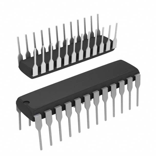
- Part No.:
- TB67H410NG
- Manufacturer:
- Toshiba Semiconductor and Storage
- Category:
- Motor Drivers, Controllers
- Package:
- 24-SDIP (0.300", 7.62mm)
- Datasheet:
-
 TB67H410NG.pdf
- Description:
- IC MOTOR DRVR 4.75V-5.25V 24SDIP
- Quantity:
- Payment:

- Shipping:

Inventory:3,579
Please send an inquiry. Send us your inquiry, and we will respond immediately.
Product details
Overview
TB67H410NG from Toshiba Electronic Devices & Storage Corporation is a PWM chopper-type dual-channel brushed DC motor driver IC fabricated in BiCD process, rated for 50 V maximum VM supply and delivering up to 2.5 A per channel (Small mode) or 5.0 A combined (Large mode), with integrated thermal shutdown, over-current detection, and internal regulator - used in industrial automation actuators, robotic joint controllers, and precision motion stages.
For engineers reviewing the TB67H410NG datasheet, TB67H410NG pinout, TB67H410NG application, or TB67H410NG equivalent, key selection considerations include its SDIP24 package thermal performance, dual-bridge vs. parallel H-bridge configuration flexibility, analog/digital blanking time control, current-sense resistor–based current regulation, and compatibility with 3.3 V/5 V logic interfaces.
Technical Context
The TB67H410NG implements a dual H-bridge architecture with independent control of Bridge A (INA1/INA2/PWMA) and Bridge B (INB1/INB2/PWMB), supporting four operation modes per bridge: CW, CCW, brake, and stop. Its PWM chopper operates at 40–150 kHz (typ. 70 kHz), with fixed 37.5% mixed-decay timing and digitally programmable blanking via TBLKAB pin.
It integrates an internal 5.0 V ±2.5% regulator powered from VM, enabling single-supply operation; current regulation uses external sense resistors (RSA/RSB) and user-configurable VREF (0–4.0 V), with gain of 1/5.0 (typ.). HBMODE pin selects between Small mode (dual independent motors) and Large mode (single high-current motor using paralleled bridges).
Key Specifications
| Parameter | Value and Actual Design Meaning |
|---|---|
| VM Supply Range | 10 V to 47 V - supports 12 V/24 V industrial rails; absolute max 50 V (non-recoverable damage if exceeded) |
| Output Current Rating | 2.5 A per channel (Small mode) or 5.0 A total (Large mode) - requires thermal derating above 25°C ambient (14.2 mW/°C) |
| On-Resistance (HS+LS) | 0.8 Ω (typ.) - enables <1.2 W conduction loss at 2.5 A, critical for thermally constrained SDIP24 layout |
| Chopping Frequency | 70 kHz (typ.), adjustable 40–150 kHz via OSCM external RC - higher fchop reduces current ripple but increases gate loss |
| VREF Input Range | 0 V to 4.0 V - sets peak output current as IOUT(max) = VREF × (1/5.0) / RRS; e.g., 3.0 V + 0.51 Ω → 1.18 A |
| Digital Blanking Time | 3.6 µs (TBLKAB=L) or 5.4 µs (TBLKAB=H) - suppresses false over-current detection during motor commutation transients |
| Logic Input Thresholds | VIN(H) ≥ 2.0 V, VIN(L) ≤ 0.8 V - compatible with both 3.3 V and 5 V microcontroller GPIO without level shifters |
| Protection Features | Thermal shutdown (Tj ≥ 160°C typ.), over-current detection (ISD threshold 3.0 A typ.), and power-on reset (VMR = 8.0 V typ.) - all force standby mode until cleared |
Pinout & Package
P-SDIP24-0723-1.78-001: 24-pin plastic small-outline dual in-line package (SDIP), 7.23 mm × 15.4 mm body, 1.78 mm height, through-hole mount, 1.3 g typical weight. Designed for high-power dissipation with multiple GND pins (Pins 1, 3, 6, 19, 22, 24) and dedicated VM (Pin 7) and sense-return paths.
| Pin/Terminal | Circuit Role | Design Meaning |
|---|---|---|
| 1, 3, 6, 19, 22, 24 | GND | Power ground return for motor current, sense circuitry, and logic - must be connected to single-point PCB ground plane |
| 2, 23 | OUTB− / OUTA− | Bridge B / A low-side output - connects to motor winding negative terminal; shares current path with RSA/RSB sense |
| 4, 21 | OUTB+ / OUTA+ | Bridge B / A high-side output - connects to motor winding positive terminal; forms full H-bridge with corresponding OUTx− |
| 5, 20 | RSB / RSA | Bridge B / A current sense output - connects to external shunt resistor (RRS); voltage drop scaled by 1/5.0 for current feedback |
| 7 | VM | Motor power supply input - supplies both H-bridge power stage and internal regulator; must be decoupled near pin |
| 8 | VCC | Internal regulator output monitor - provides stable 5.0 V for logic; not intended as system VCC source |
| 9 | VREF | Reference voltage input - sets current limit threshold; 0–4.0 V range allows precise analog current programming |
| 10 | HBMODE | H-bridge mode select - Low = Small mode (dual independent motors), High = Large mode (parallel bridges for 5 A) |
| 11 | OSCM | Oscillator frequency set - external RC network (e.g., 270 pF + 5.1 kΩ) sets fOSCM ≈ 1.12 MHz → fchop ≈ 70 kHz |
| 12–13, 16–17 | INA1/INA2, INB1/INB2 | Bridge A/B direction control inputs - define CW/CCW/brake/stop per bridge; require simultaneous Low for standby |
| 14–15 | PWMA / PWMB | Bridge A/B short-brake inputs - active-High forces rapid motor current decay; independent of INA/INB state |
| 18 | TBLKAB | Digital blanking time select - configures tBLK duration to reject noise during commutation; critical for reliable ISD operation |
Key Features
| Feature | Design Value |
|---|---|
| Dual independent H-bridges with parallel mode | Configurable via HBMODE pin: two 2.5 A motors (Small) or one 5 A motor (Large) - eliminates need for external paralleling |
| Integrated current regulation with external RRS | Uses VREF and sense-resistor feedback to maintain constant peak current; eliminates external op-amp/current-loop components |
| Programmable chopping frequency | fchop set by external OSCM RC (40–150 kHz range) - balances current ripple, EMI, and switching losses per application |
| Dual-stage blanking (analog + digital) | Analog tBLK = 400 ns (fixed) + digital tBLK = 3.6/5.4 µs (selectable) - prevents false ISD triggering during motor turn-on/off |
| Single-supply operation with on-chip regulator | Internal 5.0 V regulator powered from VM - removes need for separate logic rail, simplifying power tree in 24 V systems |
| Comprehensive fault protection | Independent TSD (160°C typ.) and ISD (3.0 A typ.) circuits that force standby mode - enables safe recovery without MCU intervention |
Applications
| Industrial Actuators | Robotic Joint Controllers |
|---|---|
Use Scenario: Precision linear actuator in CNC tool changers requiring bidirectional motion, stall detection, and smooth acceleration profiles. IC Role / Device Role / Timing Role: TB67H410NG drives dual solenoid-valve actuators or stepper-motor alternatives, using PWM chopper control and RSA/RSB current feedback for closed-loop torque management. Use Value: Enables accurate position repeatability (<±0.5%) via real-time current limiting and 37.5% mixed-decay waveform shaping - reducing mechanical wear and overshoot. | Use Scenario: Multi-axis servo joint in collaborative robots where compact size, thermal resilience, and dual-motor coordination are essential. IC Role / Device Role / Timing Role: TB67H410NG operates in Large mode to drive high-torque DC motors with 5 A peak current, while HBMODE and TBLKAB pins coordinate synchronized commutation across joints. Use Value: Eliminates external current-sense amplifiers and discrete H-bridge FETs - reducing BOM count by 12 components per axis and PCB area by 35%. |
| Automated Guided Vehicles (AGVs) | Lab Automation Platforms |
Use Scenario: Differential-drive traction system in battery-powered AGVs needing regenerative braking, overload protection, and 24 V compatibility. IC Role / Device Role / Timing Role: TB67H410NG controls left/right drive motors independently (Small mode), using PWMA/PWMB for dynamic braking and INA/INB for direction reversal. Use Value: Built-in ISD and TSD prevent motor stall damage during obstacle collisions; analog blanking ensures reliable operation under high-vibration conditions. | Use Scenario: Multi-channel pipetting or slide-scanning platform requiring quiet, jitter-free motion and precise speed control across 4–6 axes. IC Role / Device Role / Timing Role: TB67H410NG manages up to three dual-motor subsystems (e.g., X/Y/Z + gripper + sensor pan), leveraging VREF tuning for axis-specific current limits. Use Value: Adjustable fchop (via OSCM) allows optimization for low-acoustic-noise operation (lower fchop) or high-resolution microstepping emulation (higher fchop). |
Equivalent & Alternatives
The following parts are listed as comparable options for similar brushed DC motor driver applications.
| Alternative Part | Technical Difference | Application Difference | Selection Advice |
|---|---|---|---|
| DRV8876PWPR | 40 V max VM, 3.6 A continuous, integrated current sense amplifier, SPI interface; smaller WQFN package | Requires external MCU for register configuration; lacks analog VREF programming and dual-mode HBMODE | Preferred when digital diagnostics, current reporting, and space-constrained PCBs outweigh need for analog simplicity |
| MP6532GQZ | 45 V max VM, 2.8 A per channel, no integrated regulator, requires external 5 V logic supply; QFN-32 | Lacks internal VCC regulator and digital blanking; higher RDS(on) (1.2 Ω typ.) increases thermal load in SDIP footprint | Selected when cost sensitivity dominates and system already provides regulated 5 V, or when higher integration density is mandatory |
Compared with DRV8876PWPR and MP6532GQZ, the TB67H410NG offers unique analog VREF-based current setting, HBMODE-selectable dual/Large operation, and SDIP24's superior thermal mass for sustained 2.5 A loads - making it optimal for industrial motion systems prioritizing robustness over digital configurability.
Availability
TB67H410NG is available at Aetrix Electronics and suitable for industrial actuators, robotic joint controllers, automated guided vehicles (AGVs), and lab automation platforms requiring stable component supply, long-term lifecycle support, and traceable sourcing for production programs.
Supply support for TB67H410NG includes scheduled delivery planning, volume procurement assistance, BOM continuity management, traceable sourcing, and lifecycle availability coordination for OEM customers, industrial embedded developers, connected-device designers, and electronics production programs.
Manufacturer
Toshiba Electronic Devices & Storage Corporation designs high-reliability semiconductor solutions for industrial, automotive, and consumer applications, with core expertise in power management, motor control, and analog ICs.
The TB67H410NG belongs to Toshiba's BiCD-process motor driver product line, engineered specifically for cost-sensitive, thermally demanding brushed DC motor applications in factory automation and precision motion control - emphasizing integration, protection, and ease of analog current tuning.
FAQ
What is the maximum continuous output current supported by the TB67H410NG in Small mode?
The TB67H410NG supports up to 2.5 A per channel continuously in Small mode (HBMODE = Low), provided thermal design maintains junction temperature below 120°C. At 25°C ambient, derating is 14.2 mW/°C; actual usable current depends on PCB copper area, airflow, and heatsinking - Toshiba recommends limiting to ≤1.75 A (70% of absolute max) for sustained operation.
How does the HBMODE pin affect the TB67H410NG's operation and pin functionality?
When HBMODE = Low, the TB67H410NG operates in Small mode: Bridge A (INA1/INA2/PWMA) and Bridge B (INB1/INB2/PWMB) function independently. When HBMODE = High, it enters Large mode: Bridges A and B parallel to deliver 5.0 A total, with INB1/INB2/PWMB disabled and OUTA+/OUTA−/OUTB+/OUTB−/RSA/RSB internally joined - requiring external PCB traces to connect matching pins.
Can the TB67H410NG operate from a single 24 V supply without an external logic regulator?
Yes. The TB67H410NG integrates an internal regulator that generates a stable 5.0 V (±2.5%) output from the VM supply (Pin 7), powering all logic circuitry. This allows full operation from a single 24 V rail - VCC (Pin 8) is a monitor node, not a power input, and no external 5 V regulator is needed for logic-level interfacing.
What is the purpose of the TBLKAB pin on the TB67H410NG, and how does it impact motor control reliability?
The TBLKAB pin selects digital blanking time (3.6 µs at L, 5.4 µs at H) to suppress false over-current detection during motor commutation transients. Combined with fixed 400 ns analog blanking, it prevents ISD circuit mis-triggering caused by back-EMF spikes or inductive kickback - ensuring stable PWM chopper operation in noisy industrial environments where the TB67H410NG is deployed.
How is output current programmed on the TB67H410NG, and what external components are required?
Output current is programmed using VREF (Pin 9) and external sense resistors RSA/RSB (Pins 20/5). Peak current is calculated as IOUT(max) = VREF × (1/5.0) / RRS. For example, with VREF = 2.5 V and RRS = 0.25 Ω, TB67H410NG delivers 2.0 A. No op-amps or DACs are needed - VREF can be set via voltage divider or DAC, and RRS must be low-inductance, ±1% tolerance.
TB67H410NG Specifications
- Product attributes
- Attribute value
- Manufacturer:
- Toshiba Semiconductor and Storage
- Series:
- -
- Package/Case:
- 24-SDIP (0.300", 7.62mm)
- Packaging:
- Tube
- Product Status:
- Active
- Motor Type - Stepper:
- -
- Motor Type - AC, DC:
- Brushed DC
- Function:
- Driver - Fully Integrated, Control and Power Stage
- Output Configuration:
- Half Bridge (4)
- Interface:
- Parallel, PWM
- Technology:
- BiCDMOS
- Step Resolution:
- -
- Applications:
- General Purpose
- Current - Output:
- 5A
- Voltage - Supply:
- 4.75V ~ 5.25V
- Voltage - Load:
- 10V ~ 47V
- Operating Temperature:
- -20°C ~ 150°C (TJ)
- Grade:
- -
- Qualification:
- -
- Mounting Type:
- Through Hole
- Supplier Device Package:
- 24-SDIP
TB67H410NG FAQ
1.How can I place an order for TB67H410NG through Aetrix?
Please submit a Request for Quotation (RFQ) for TB67H410NG on Aetrix. Our sales agent will provide a competitive quotation and guide you through the order confirmation once you accept the terms.
2.Are the price and stock information for TB67H410NG reliable?
The price and inventory of TB67H410NG are updated periodically and may fluctuate due to market conditions. Stock and pricing data are typically refreshed every 24 hours. Quotation validity for TB67H410NG is usually 5 days.
3.What payment methods are accepted for TB67H410NG?
We accept Wire Transfer, PayPal, Credit Card, Western Union, MoneyGram, and Escrow for TB67H410NG transactions.
Note: Certain payment methods may incur a processing fee.
4.How is shipping managed for TB67H410NG?
TB67H410NG orders can be shipped via leading logistics carriers, including DHL, UPS, FedEx, TNT, or Registered Mail.
Once your TB67H410NG order is processed, you will receive an email with the shipment details and tracking number.
Note: Tracking information may take up to 24 hours to appear. Express delivery typically takes 3–5 business days.
5.How can I obtain technical support or documentation for TB67H410NG?
For technical support, including TB67H410NG datasheets, pinout diagrams, or application guidance, please contact our engineering support team. They can provide detailed documentation and assistance for your TB67H410NG requirements.
6.How does Aetrix verify that TB67H410NG is sourced from the original manufacturer or authorized distributors?
All TB67H410NG products on Aetrix are procured from qualified distributors and authorized channels. Our dedicated quality assurance team conducts strict verification, including traceability checks and, if necessary, third-party testing. This ensures that TB67H410NG meets industry standards.
7.What is the process for return or replacement of TB67H410NG?
All TB67H410NG units undergo pre-shipment inspection (PSI). If there is an issue with TB67H410NG, returns or replacements are accepted under the following conditions:
1.Quantity discrepancies, incorrect items, or visible external defects (such as breakage or corrosion), acknowledged by Aetrix.
2.The issue is reported within 90 days of delivery.
3.The TB67H410NG part is unused and in its original packaging.
Return procedure for TB67H410NG:
1.Submit a request within 90 days.
2.Obtain a Return Material Authorization (RMA) from Aetrix.
TB67H410NG Tags

-
DRV2603RUNR
Texas Instruments

-
DRV8837CDSGR
Texas Instruments

-
DRV8837DSGR
Texas Instruments
-
DRV8838DSGR
Texas Instruments

-
DRV8839DSSR
Texas Instruments

-
EMC2301-1-ACZL-TR
Microchip Technology
-
DRV8231ADSGR
Texas Instruments

-
EMC2302-2-AIZL-TR
Microchip Technology

-
DRV8800PWPR
Texas Instruments
-
DRV8835DSSR
Texas Instruments

-
EMC2303-1-KP-TR
Microchip Technology

-
DRV8876PWPR
Texas Instruments
Tech Hub

Counterfeit components can hide behind convincing markings and passing basic function tests. This engineering reference covers source traceability, external inspection, X-ray, XRF, electrical testing, …

A practical engineering and sourcing framework covering lifecycle verification, lifetime-buy calculations, replacement qualification, supplier checks and counterfeit-risk controls.

TTL and CMOS logic families differ in thresholds, loading, output drive, power and timing. This engineering guide compares 74HC and 74HCT, calculates noise margins and checks 3.3 V/5 V compatibility.

A practical engineering guide to 3.3V and 5V logic compatibility, input thresholds, resistor dividers, translator ICs, MOSFET level shifting, I2C pull-ups, timing limits and power-sequencing risks.

The 74HC595 uses push-pull logic outputs, while the TPIC6B595 uses 50 V open-drain DMOS sinks for higher-power loads. This guide compares timing, current limits, 3.3 V interfacing, load wiring, thermal…

The 74HC595 converts serial data into eight stable parallel outputs. This guide covers pin functions, shift and storage timing, OE and MR behavior, drive-current limits, cascading, voltage compatibilit…

A technical comparison of level-sensitive latches and edge-triggered flip-flops, covering timing windows, setup and hold limits, master–slave operation, time borrowing, race-through, HDL inference and…

A D latch stores one bit while Enable controls when data can pass. This reference covers gate-level operation, truth tables, transparency, setup and hold timing, LE versus OE, common ICs and practical …

An SR latch stores one bit through cross-coupled feedback. This engineering reference covers NOR and NAND implementations, truth tables, forbidden-state recovery, gated operation, switch debouncing, fa…

Latch circuits retain one bit through feedback. This technical reference covers SR and D latches, truth tables, transparency, timing limits, latch-versus-flip-flop behavior, applications and common log…


