
 My Inquiry
 My Account


Toshiba Semiconductor and Storage TB67S102AFNG,EL
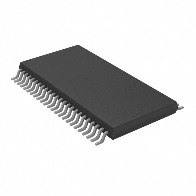
- Part No.:
- TB67S102AFNG,EL
- Manufacturer:
- Toshiba Semiconductor and Storage
- Category:
- Motor Drivers, Controllers
- Package:
- 48-TFSOP (0.240", 6.10mm Width) Exposed Pad
- Datasheet:
-
 TB67S102AFNG,EL.pdf
- Description:
- IC MOTOR DRIVER BIPOLAR 48HTSSOP
- Quantity:
- Payment:

- Shipping:

Inventory:4,492
Please send an inquiry. Send us your inquiry, and we will respond immediately.
Product details
Overview
TB67S102AFNG,EL from Toshiba is a clock-in controlled bipolar stepping motor driver IC fabricated in BiCD process, delivering 50 V/4.0 A rating, PWM chopper-based constant-current drive, full/half/quarter-step resolution, and integrated Advanced Dynamic Mixed Decay (ADMD) current control for precision motion systems in industrial automation and CNC equipment.
For engineers reviewing the TB67S102AFNG,EL datasheet, TB67S102AFNG,EL pinout, TB67S102AFNG,EL application, or TB67S102AFNG,EL equivalent, key selection criteria include its HTSSOP48 package thermal performance, dual-channel 1.5 A typical output current (3.0 A max), 0.49 Ω typical high-side + low-side ON-resistance, ADMD decay mode behavior, and OSCM-set chopper frequency range of 40–150 kHz.
Technical Context
The TB67S102AFNG,EL implements a clock-driven step sequencer with CW/CCW direction control and DMODE1/DMODE2-configurable resolution (full/half/quarter). Its internal oscillator (OSCM) sets chopper frequency via external RC network, with fchop = fOSCM / 16 - typically 70 kHz at 1.12 MHz OSCM.
Current regulation uses dual RS-sense inputs (RSA/RSB) and VREFA/VREFB reference voltage inputs, enabling independent channel current setting via Iout(max) = Vref × (1/5.0) / RS. Protection includes thermal shutdown (TSD at 145–175°C), overcurrent shutdown (ISD at 4.1–5.7 A), and power-on reset (POR).
Key Specifications
| Parameter | Value and Actual Design Meaning |
|---|---|
| Motor Supply Voltage | 10–47 V - supports 24 V nominal industrial rails; absolute max 50 V avoids destructive overvoltage |
| Output Current Rating | 1.5 A typ / 3.0 A max - derated from 4.0 A absolute max due to thermal limits in HTSSOP48 package |
| ON-Resistance (HS+LS) | 0.49 Ω typ - enables <1.2 W conduction loss per channel at 1.5 A, critical for thermal management |
| Chopper Frequency Range | 40–150 kHz - adjustable via OSCM pin RC network; 70 kHz typical balances ripple vs. switching loss |
| Step Resolution Modes | Full / Half (Type A) / Quarter - selected by DMODE1/DMODE2 logic levels; quarter-step enables 4× microstepping resolution |
| Logic Input Thresholds | VIN(H) ≥ 2.0 V, VIN(L) ≤ 0.8 V - compatible with 3.3 V and 5 V CMOS controllers without level shifting |
| Protection Functions | TSD (145–175°C), ISD (4.1–5.7 A), POR - autonomous shutdown prevents latch-up or permanent damage during fault events |
Pinout & Package
HTSSOP48-P-300-0.50 package: 48-pin thermally enhanced thin shrink small outline package with exposed pad (mounted to PCB GND for heat dissipation); 0.5 mm pitch, 7.0 × 7.0 mm body size, 0.21 g typical weight.
| Pin/Terminal | Circuit Role | Design Meaning |
|---|---|---|
| 1, 11, 20, 24, 25, 29, 46 | GND | Multiple ground terminals - must be connected to common PCB GND plane; exposed pad also tied to GND for thermal conduction |
| 3, 44 | CW/CCW | Direction control input - high = clockwise, low = counterclockwise; determines phase sequence of OUTA/OUTB outputs |
| 4, 45 | MO | Electric angle monitor output - open-drain digital signal indicating motor electrical angle position for closed-loop feedback |
| 5, 7, 46, 47 | DMODE1 / DMODE2 | Step resolution select inputs - configure full/half/quarter step or standby mode; require RESET assertion when changing |
| 8, 43 | OSCM | Oscillator frequency set pin - connects external RC (e.g., 5.1 kΩ + 270 pF) to define chopper frequency (fchop = fOSCM/16) |
| 13–14, 35–36 | RSA / RSB | Current sense inputs - connect to low-side sense resistors (e.g., 0.51 Ω); enable precise per-channel current regulation |
| 16–17, 22–23, 26–27, 32–33 | OUTA+/OUTA− / OUTB+/OUTB− | H-bridge motor outputs - paralleled pins per terminal increase current capacity and reduce trace inductance |
| 39 | VM | Motor power supply input - accepts 10–47 V; requires local bulk capacitance and low-ESR decoupling near device |
| 41–42 | VREFB / VREFA | Reference voltage inputs - set peak current via Iout = Vref × (1/5.0) / RS; range 0–3.6 V supports fine-grained torque control |
Key Features
| Feature | Design Value |
|---|---|
| Advanced Dynamic Mixed Decay (ADMD) | Automatically switches between fast/slow decay based on current error vs. ADMD threshold - minimizes torque ripple while suppressing heat generation |
| Dual-channel independent current setting | VREFA/VREFB inputs allow asymmetric current profiles (e.g., higher hold vs. lower run current) without external DACs |
| Integrated VCC regulator | Internal 5.0 V ±2.5% regulator powers logic circuitry - eliminates need for external 5 V rail; draws 2.5–5 mA ICC |
| Multi-package compatibility | Same functional design across HSOP28, QFN48, and HTSSOP48 - TB67S102AFNG,EL offers best thermal performance for high-current applications |
| Built-in fault detection | Simultaneous TSD, ISD, and POR monitoring - asserts safe shutdown before junction temperature exceeds 150°C or current hits 5.7 A |
Applications
| Industrial CNC Positioning | Medical Infusion Pump Drive |
|---|---|
Use Scenario: Precise linear actuation in multi-axis CNC milling machines requiring sub-micron repeatability and smooth velocity profiling. IC Role / Device Role / Timing Role: Bipolar stepper driver executing clock-synchronized step commands; MO pin provides real-time angle feedback for stall detection. Use Value: ADMD decay ensures minimal current ripple at 70 kHz chopper frequency, preserving torque linearity across 0–1000 PPS range without external compensation. | Use Scenario: Silent, low-vibration motor control in portable infusion pumps where audible noise and mechanical resonance must be minimized. IC Role / Device Role / Timing Role: Constant-current H-bridge driver with quarter-step resolution enabling fine flow-rate granularity (e.g., 0.01 mL/hr increments). Use Value: 0.49 Ω ON-resistance reduces conduction loss to <1.2 W at 1.5 A, limiting self-heating in sealed enclosures without active cooling. |
| Automated Optical Inspection (AOI) Stage | Lab Automation Robotic Arm Joint |
Use Scenario: High-speed XY stage movement in semiconductor wafer inspection systems requiring rapid acceleration/deceleration without step loss. IC Role / Device Role / Timing Role: Clock-driven stepper controller accepting FPGA-generated CLK pulses; ENABLE pin enables dynamic power gating between motion phases. Use Value: 100 ns CLK-to-output propagation delay (tpLH/tpHL) ensures deterministic timing alignment with vision trigger signals for synchronized image capture. | Use Scenario: Compact joint actuation in collaborative robotic arms where space-constrained PCB layout demands high integration density. IC Role / Device Role / Timing Role: Dual-H-bridge motor driver with integrated current sensing and thermal protection - replaces discrete MOSFET + op-amp + comparator solution. Use Value: HTSSOP48 package with exposed pad achieves 1.3 W power dissipation capability - sustains 1.5 A continuous per channel under 60°C ambient with 2 oz copper. |
Equivalent & Alternatives
The following parts are listed as comparable options for similar bipolar stepping motor driver applications.
| Alternative Part | Technical Difference | Application Difference | Selection Advice |
|---|---|---|---|
| STSPIN820TR | 45 V/3.5 A rating; integrated current sense amplifier; SPI interface instead of clock/step logic | Requires microcontroller firmware for step sequencing; lacks MO angle monitor output | Prefer when system already uses SPI bus and needs diagnostic telemetry over hardware simplicity |
| MP6500GQZ | 36 V/2.5 A rating; fixed 1/8-step resolution; no OSCM frequency tuning - fixed 30 kHz chopper | Lower thermal margin; no quarter-step mode; simpler BOM but less flexible current control | Prefer for cost-sensitive, low-power applications where 2.5 A and fixed decay suffice |
Compared with STSPIN820TR and MP6500GQZ, TB67S102AFNG,EL delivers superior thermal headroom (1.3 W PD), hardware-based clock-step simplicity, and unique MO angle monitoring - making it optimal for deterministic, embedded motion control without host processor overhead.
Availability
TB67S102AFNG,EL is available at Aetrix Electronics and suitable for industrial CNC positioning, medical infusion pump drive, automated optical inspection stages, and lab automation robotic arm joints requiring stable component supply and long-term production continuity.
Supply support for TB67S102AFNG,EL includes scheduled delivery planning, volume procurement assistance, BOM continuity management, traceable sourcing, and lifecycle availability coordination for OEM customers, industrial embedded developers, connected-device designers, and electronics production programs.
Manufacturer
Toshiba Electronic Devices & Storage Corporation designs high-reliability analog and power ICs for industrial, automotive, and consumer applications, with deep expertise in BiCD process technology and motor control integration.
TB67S102AFNG,EL belongs to Toshiba's TB67S series of integrated bipolar stepper drivers, engineered specifically for high-voltage, high-current motion control in space- and thermally-constrained industrial equipment.
FAQ
What is the maximum continuous output current supported by TB67S102AFNG,EL in its HTSSOP48 package?
TB67S102AFNG,EL supports 1.5 A typical continuous output current per channel under standard conditions (Ta = 25°C, 2-layer PCB, 2 oz copper). The absolute maximum rating is 4.0 A, but thermal limits in the HTSSOP48 package constrain practical operation to ≤3.0 A with aggressive heatsinking. Derating is required above 60°C ambient temperature per the datasheet's thermal resistance (θJA) curve.
How does the OSCM pin configure chopper frequency in TB67S102AFNG,EL?
The OSCM pin in TB67S102AFNG,EL connects to an external RC network (e.g., 5.1 kΩ resistor + 270 pF capacitor) to set the internal oscillator frequency (fOSCM), which is then divided by 16 to determine chopper frequency (fchop = fOSCM / 16). With typical values, fOSCM ≈ 1.12 MHz yields fchop ≈ 70 kHz - balancing current ripple suppression against switching losses and thermal rise.
Does TB67S102AFNG,EL require external current sense resistors, and how are they connected?
Yes, TB67S102AFNG,EL requires two external low-value current sense resistors - one for each motor phase - connected between the RSA/RSB pins and GND. These resistors (e.g., 0.51 Ω) convert motor current into a voltage sensed by the IC's internal comparators. The peak current is calculated as Iout(max) = Vref × (1/5.0) / RS, where Vref is applied to VREFA/VREFB pins.
What protection features are built into TB67S102AFNG,EL, and how do they respond to faults?
TB67S102AFNG,EL integrates thermal shutdown (TSD), overcurrent shutdown (ISD), and power-on reset (POR). TSD triggers at 145–175°C junction temperature, forcing standby mode until VM is cycled or DMODE enters standby. ISD activates at 4.1–5.7 A output current, latching off outputs until POR or DMODE reset. Both functions prevent catastrophic failure but require external fusing for sustained fault conditions.
Can TB67S102AFNG,EL operate with a 3.3 V logic supply, or does it require 5 V?
TB67S102AFNG,EL accepts 3.3 V logic inputs reliably: its VIN(H) threshold is 2.0 V min and VIN(L) is 0.8 V max, fully compatible with standard 3.3 V CMOS outputs. The internal VCC regulator generates a stable 5.0 V ±2.5% rail for internal logic - no external 5 V supply is needed. However, VCC pin must be decoupled with a 1 µF ceramic capacitor to GND.
TB67S102AFNG,EL Specifications
- Product attributes
- Attribute value
- Manufacturer:
- Toshiba Semiconductor and Storage
- Series:
- -
- Package/Case:
- 48-TFSOP (0.240", 6.10mm Width) Exposed Pad
- Packaging:
- Tape & Reel (TR)
- Product Status:
- Active
- Motor Type - Stepper:
- Bipolar
- Motor Type - AC, DC:
- -
- Function:
- Driver - Fully Integrated, Control and Power Stage
- Output Configuration:
- Half Bridge (4)
- Interface:
- Parallel
- Technology:
- Power MOSFET
- Step Resolution:
- 1, 1/2, 1/4
- Applications:
- General Purpose
- Current - Output:
- 3A
- Voltage - Supply:
- 4.75V ~ 5.25V
- Voltage - Load:
- 10V ~ 47V
- Operating Temperature:
- -20°C ~ 150°C (TJ)
- Grade:
- -
- Qualification:
- -
- Mounting Type:
- Surface Mount
- Supplier Device Package:
- 48-HTSSOP
TB67S102AFNG,EL FAQ
1.How can I place an order for TB67S102AFNG,EL through Aetrix?
Please submit a Request for Quotation (RFQ) for TB67S102AFNG,EL on Aetrix. Our sales agent will provide a competitive quotation and guide you through the order confirmation once you accept the terms.
2.Are the price and stock information for TB67S102AFNG,EL reliable?
The price and inventory of TB67S102AFNG,EL are updated periodically and may fluctuate due to market conditions. Stock and pricing data are typically refreshed every 24 hours. Quotation validity for TB67S102AFNG,EL is usually 5 days.
3.What payment methods are accepted for TB67S102AFNG,EL?
We accept Wire Transfer, PayPal, Credit Card, Western Union, MoneyGram, and Escrow for TB67S102AFNG,EL transactions.
Note: Certain payment methods may incur a processing fee.
4.How is shipping managed for TB67S102AFNG,EL?
TB67S102AFNG,EL orders can be shipped via leading logistics carriers, including DHL, UPS, FedEx, TNT, or Registered Mail.
Once your TB67S102AFNG,EL order is processed, you will receive an email with the shipment details and tracking number.
Note: Tracking information may take up to 24 hours to appear. Express delivery typically takes 3–5 business days.
5.How can I obtain technical support or documentation for TB67S102AFNG,EL?
For technical support, including TB67S102AFNG,EL datasheets, pinout diagrams, or application guidance, please contact our engineering support team. They can provide detailed documentation and assistance for your TB67S102AFNG,EL requirements.
6.How does Aetrix verify that TB67S102AFNG,EL is sourced from the original manufacturer or authorized distributors?
All TB67S102AFNG,EL products on Aetrix are procured from qualified distributors and authorized channels. Our dedicated quality assurance team conducts strict verification, including traceability checks and, if necessary, third-party testing. This ensures that TB67S102AFNG,EL meets industry standards.
7.What is the process for return or replacement of TB67S102AFNG,EL?
All TB67S102AFNG,EL units undergo pre-shipment inspection (PSI). If there is an issue with TB67S102AFNG,EL, returns or replacements are accepted under the following conditions:
1.Quantity discrepancies, incorrect items, or visible external defects (such as breakage or corrosion), acknowledged by Aetrix.
2.The issue is reported within 90 days of delivery.
3.The TB67S102AFNG,EL part is unused and in its original packaging.
Return procedure for TB67S102AFNG,EL:
1.Submit a request within 90 days.
2.Obtain a Return Material Authorization (RMA) from Aetrix.
TB67S102AFNG,EL Tags

-
DRV2603RUNR
Texas Instruments

-
DRV8837CDSGR
Texas Instruments

-
DRV8837DSGR
Texas Instruments
-
DRV8838DSGR
Texas Instruments

-
DRV8839DSSR
Texas Instruments

-
EMC2301-1-ACZL-TR
Microchip Technology
-
DRV8231ADSGR
Texas Instruments

-
EMC2302-2-AIZL-TR
Microchip Technology

-
DRV8800PWPR
Texas Instruments
-
DRV8835DSSR
Texas Instruments

-
EMC2303-1-KP-TR
Microchip Technology

-
DRV8876PWPR
Texas Instruments
Tech Hub

Counterfeit components can hide behind convincing markings and passing basic function tests. This engineering reference covers source traceability, external inspection, X-ray, XRF, electrical testing, …

A practical engineering and sourcing framework covering lifecycle verification, lifetime-buy calculations, replacement qualification, supplier checks and counterfeit-risk controls.

TTL and CMOS logic families differ in thresholds, loading, output drive, power and timing. This engineering guide compares 74HC and 74HCT, calculates noise margins and checks 3.3 V/5 V compatibility.

A practical engineering guide to 3.3V and 5V logic compatibility, input thresholds, resistor dividers, translator ICs, MOSFET level shifting, I2C pull-ups, timing limits and power-sequencing risks.

The 74HC595 uses push-pull logic outputs, while the TPIC6B595 uses 50 V open-drain DMOS sinks for higher-power loads. This guide compares timing, current limits, 3.3 V interfacing, load wiring, thermal…

The 74HC595 converts serial data into eight stable parallel outputs. This guide covers pin functions, shift and storage timing, OE and MR behavior, drive-current limits, cascading, voltage compatibilit…

A technical comparison of level-sensitive latches and edge-triggered flip-flops, covering timing windows, setup and hold limits, master–slave operation, time borrowing, race-through, HDL inference and…

A D latch stores one bit while Enable controls when data can pass. This reference covers gate-level operation, truth tables, transparency, setup and hold timing, LE versus OE, common ICs and practical …

An SR latch stores one bit through cross-coupled feedback. This engineering reference covers NOR and NAND implementations, truth tables, forbidden-state recovery, gated operation, switch debouncing, fa…

Latch circuits retain one bit through feedback. This technical reference covers SR and D latches, truth tables, transparency, timing limits, latch-versus-flip-flop behavior, applications and common log…


