
 My Inquiry
 My Account


Toshiba Semiconductor and Storage TB67S522FTAG,EL
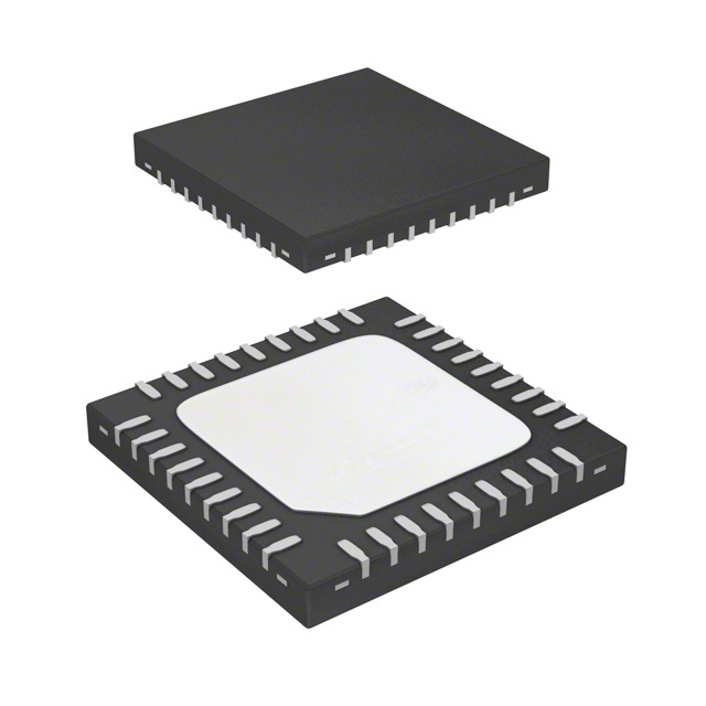
- Part No.:
- TB67S522FTAG,EL
- Manufacturer:
- Toshiba Semiconductor and Storage
- Category:
- Motor Drivers, Controllers
- Package:
- 36-WFQFN Exposed Pad
- Datasheet:
-
 TB67S522FTAG,EL.pdf
- Description:
- IC MOTOR DRIVER 36WQFN
- Quantity:
- Payment:

- Shipping:

Inventory:1,234
Please send an inquiry. Send us your inquiry, and we will respond immediately.
Product details
Overview
TB67S522FTAG from Toshiba Electronic Devices & Storage Corporation is a PWM chopper-type two-phase bipolar stepping motor driver IC rated for 40 V and 2.8 A per channel, featuring integrated mixed-decay control, thermal shutdown (TSD), over-current detection (ISD), and a built-in VCC regulator enabling single-VM supply operation in precision motion control systems.
For engineers reviewing the TB67S522FTAG datasheet, TB67S522FTAG pinout, TB67S522FTAG application, or TB67S522FTAG equivalent, key selection considerations include its 36-pin WQFN package, support for full/half/quarter-step resolution via D_MODE1/D_MODE2, external OSCM frequency tuning, and dual-channel current sensing via RS_A1/RS_A2 and RS_B1/RS_B2 pins.
Technical Context
The TB67S522FTAG implements a two-channel H-bridge output stage with BiCD process low on-resistance (0.53 Ω typical, H+L), mixed-decay current control using internal chopping oscillator (fchop = fOSCM/16), and step-angle progression synchronized to CLK_IN rising edges. Its current regulation uses VREF_A/VREF_B bias inputs and external sense resistors (RS_A1/RS_A2, RS_B1/RS_B2) to set peak output current per phase.
Functional logic includes CW/CCW direction control, ENABLE-driven output enable/disable, RESET-initiated electrical angle initialization, and MO_OUT monitor pin for real-time angle tracking. The device integrates VMR detection, POR, and protection circuits-TSD (trip at 140–170 °C), ISD (4.0 A typical trip threshold), and noise-rejection blanking (300 ns typical).
Key Specifications
| Parameter | Value and Actual Design Meaning |
|---|---|
| Supply Voltage (VM) | 10–35 V typical operating range; supports up to 40 V absolute max - enables compatibility with 24 V industrial motor rails. |
| Output Current (per channel) | 1.5–2.5 A typical continuous; 2.8 A absolute max - requires thermal derating above 25 °C ambient (32.8 mW/°C on 4-layer PCB). |
| Chopping Frequency (fchop) | 40–150 kHz operational range - adjustable via OSCM pin (270 pF + 3.6 kΩ yields ~100 kHz) to balance ripple reduction vs. switching loss. |
| Step Resolution Modes | Full, half, and quarter step via D_MODE1/D_MODE2 logic inputs - provides 400, 800, or 1600 steps/rev with torque retention down to 71% in quarter-step mode. |
| On-Resistance (H+L) | 0.53 Ω typical (25 °C) - minimizes conduction loss and heat generation at 2 A load (P ≈ 2.12 W per H-bridge). |
| Protection Features | Integrated TSD (150 °C nominal trip), ISD (4.0 A trip), and POR - eliminates need for external fault-handling circuitry in compact designs. |
| Logic Supply | VCC internally regulated from VM - allows single-supply system architecture without auxiliary 5 V rail. |
Pinout & Package
Package: P-WQFN36-0606-0.50-002 - 6 mm × 6 mm, 0.5 mm pitch, 36-pin wettable flank QFN with exposed thermal pad (0.14 g typical weight). Requires careful PCB layout: dedicated GND plane, short high-current traces (VM, OUT_Ax±, OUT_Bx±), and single-point grounding per datasheet layout guidance.
| Pin/Terminal | Circuit Role | Design Meaning |
|---|---|---|
| CLK_IN (1) | Clock input | Rising-edge-triggered step advance - determines motor rotation speed and position resolution. |
| ENABLE (2) | Output enable control | Drives both H-bridges into high-impedance state when LOW - enables power-gating during idle periods. |
| RESET (3) | Electrical angle reset | Forces initial motor phase alignment (e.g., 45° offset in full-step mode) and clears MO_OUT status. |
| RS_A1/RS_A2 (6,7) | Current sense inputs (A) | Connect to same external sense resistor - sets A-channel peak current via VREF_A and RSENSE. |
| OUT_A1+/OUT_A2+ (8,9) | A-phase high-side outputs | Drive A-coil terminals in parallel configuration - supports higher current delivery and reduced trace inductance. |
| OUT_A1-/OUT_A2- (11,12) | A-phase low-side outputs | Complement high-side outputs in H-bridge topology - enables bidirectional current flow through A coil. |
| RS_B1/RS_B2 (21,22) | Current sense inputs (B) | Identical function to RS_A1/A2 for B-phase - allows independent or matched current tuning per channel. |
| VM (23) | Motor power supply input | Primary high-voltage rail (up to 40 V) powering both H-bridges and internal regulators - requires bulk capacitance (100 µF typical). |
| VREF_A/VREF_B (31,30) | Reference voltage inputs | Set per-channel current limit via VREF/5.0 × 1/RSENSE - e.g., 3.0 V + 0.51 Ω → 1.18 A peak. |
| OSCM (32) | Oscillator frequency setting | RC-tuned node (270 pF + 3.6 kΩ) defining fOSCM - directly scales chopper frequency (fchop = fOSCM/16). |
| CW/CCW (33) | Direction control | H = clockwise, L = counter-clockwise - determines sign of incremental step angle in decoder logic. |
| MO_OUT (34) | Monitor output | Open-drain signal reflecting real-time electrical angle - used for closed-loop verification or synchronization. |
| D_MODE1/D_MODE2 (35,36) | Step resolution select | Binary-encoded inputs selecting full/half/quarter step or standby - requires RESET assertion before mode change. |
Key Features
| Feature | Design Value |
|---|---|
| PWM constant-current drive | Enables precise microstepping with stable torque across speed range by regulating coil current via chopper feedback. |
| Mixed-decay current control | Combines slow and fast decay phases (37.5% fast timing) to minimize current ripple while limiting back-EMF voltage spikes. |
| Single-VM supply architecture | VCC regulator derives 5 V logic supply from VM - eliminates need for separate 5 V rail and simplifies board power design. |
| Configurable step resolution | Hardware-selectable full/half/quarter step via D_MODE pins - delivers 400–1600 steps/rev without firmware changes. |
| Integrated protection suite | TSD, ISD, and POR operate autonomously - prevents latch-up or destruction during overload, short-circuit, or thermal runaway events. |
Applications
| Industrial CNC Positioning | Medical Infusion Pump Actuation |
|---|---|
Use Scenario: High-accuracy linear motion control in multi-axis CNC tooling where sub-micron repeatability and smooth acceleration profiles are required. IC Role / Device Role / Timing Role: Two-phase bipolar stepper driver executing microstepped position commands via CLK_IN and CW/CCW, with MO_OUT providing real-time angle feedback for error correction. Use Value: Mixed-decay control reduces audible motor noise and vibration at low speeds; 0.53 Ω on-resistance minimizes self-heating during extended dwell periods. | Use Scenario: Precise volumetric dosing in hospital-grade infusion pumps, where flow rate stability and fail-safe shutdown are critical for patient safety. IC Role / Device Role / Timing Role: Motor driver enforcing strict current limits (via VREF_A/B and RS pins) and triggering immediate ISD/TSD shutdown upon occlusion or stall detection. Use Value: Integrated ISD (4.0 A trip) and TSD (150 °C) eliminate need for external current monitors or thermal sensors - reducing BOM count and validation effort. |
| Automated Optical Inspection (AOI) Stage | 3D Printer Extruder Motion Control |
Use Scenario: Sub-pixel camera positioning in semiconductor wafer inspection systems requiring jitter-free motion and rapid direction reversal. IC Role / Device Role / Timing Role: Stepper controller accepting high-frequency CLK_IN (up to 100 kHz) and responding to CW/CCW toggles within nanoseconds to reverse motion direction mid-scan. Use Value: 100 ns typical output rise/fall time (tr/tf) and 1 µs CLK-to-output propagation delay ensure tight timing margins in high-speed scanning sequences. | Use Scenario: X/Y gantry movement in desktop 3D printers where compact size, thermal efficiency, and silent operation improve user experience. IC Role / Device Role / Timing Role: Bipolar driver implementing quarter-step resolution (1600 steps/rev) to achieve 0.01 mm layer positioning accuracy with standard NEMA17 motors. Use Value: Quarter-step mode retains 71% torque per step while doubling positional resolution - enabling finer Z-axis layer control without mechanical gear reduction. |
Equivalent & Alternatives
The following parts are listed as comparable options for similar bipolar stepping motor driver applications.
| Alternative Part | Technical Difference | Application Difference | Selection Advice |
|---|---|---|---|
| STSPIN820 | 45 V/3 A rating; integrated current sense amplifier; SPI interface for parameter programming; no external OSCM tuning. | Requires SPI host controller; lacks MO_OUT angle monitor; better suited for digitally managed motion systems. | Choose STSPIN820 when programmable decay modes, diagnostics, and embedded current sensing outweigh need for analog OSCM tuning and angle monitoring. |
| DRV8825 | 45 V/2.2 A rating; fixed 1/32 microstep mode; no mixed-decay control; requires external VDD rail. | Lacks thermal/current monitoring outputs; limited to fixed microstepping; higher external component count due to dual-supply requirement. | Choose DRV8825 only for cost-sensitive, low-complexity applications where full/half/quarter-step flexibility and integrated protection are not required. |
Compared with STSPIN820 and DRV8825, the TB67S522FTAG uniquely combines analog OSCM frequency tuning, real-time MO_OUT angle monitoring, and hardware-selectable step resolution - making it optimal for compact, single-supply, analog-controlled stepper systems demanding predictable thermal behavior and minimal external components.
Availability
TB67S522FTAG is available at Aetrix Electronics and suitable for industrial CNC positioning, medical infusion pump actuation, automated optical inspection stages, and 3D printer extruder motion control requiring stable component supply, long-term lifecycle support, and consistent parametric performance across production batches.
Supply support for TB67S522FTAG includes scheduled delivery planning, volume procurement assistance, BOM continuity management, traceable sourcing, and lifecycle availability coordination for OEM customers, industrial embedded developers, connected-device designers, and electronics production programs.
Manufacturer
Toshiba Electronic Devices & Storage Corporation is a Japanese semiconductor manufacturer specializing in power management, motor drivers, and analog ICs for industrial, automotive, and consumer applications.
The TB67S522FTAG belongs to Toshiba's TB67S series of bipolar stepper drivers, designed specifically for compact, thermally constrained motion control systems requiring high current density, integrated protection, and flexible microstepping without microcontroller overhead.
FAQ
What is the maximum continuous output current per channel for the TB67S522FTAG under typical operating conditions?
The TB67S522FTAG supports 1.5–2.5 A per channel under typical operating conditions (Ta = 0–85 °C, VM = 24 V), with 2.8 A specified as absolute maximum. Sustained 2.5 A operation requires adequate PCB thermal design - e.g., 4-layer board with 100 mm × 110 mm copper area and thermal pad soldering. At 25 °C ambient, power dissipation must be derated by 32.8 mW/°C above that point. Real-world current capability depends on heatsinking, airflow, and duty cycle - always verify junction temperature stays below 120 °C in final layout. The TB67S522FTAG datasheet specifies 2 A as a conservative thermal design target.
How does the TB67S522FTAG implement mixed-decay current control, and what is its practical benefit?
The TB67S522FTAG implements mixed-decay control by alternating between slow and fast decay phases within each chopper cycle - specifically, 37.5% of fchop time in fast decay and 62.5% in slow decay. This balances low current ripple (reducing motor vibration and acoustic noise) against excessive back-EMF voltage spikes during fast decay. The result is smoother low-speed operation and improved torque consistency across speed ranges. Unlike pure slow-decay drivers, this approach avoids current lag at higher frequencies; unlike pure fast-decay drivers, it prevents damaging voltage overshoot on the VM rail. The TB67S522FTAG's fixed 37.5% ratio is optimized for general-purpose bipolar stepper loads without requiring external tuning.
Can the TB67S522FTAG operate from a single power supply, and how is the logic voltage generated?
Yes, the TB67S522FTAG operates from a single VM supply (10–35 V typical) thanks to its integrated VCC voltage regulator. This internal regulator derives a stable ~5 V logic supply from the VM rail and powers all digital circuitry, including input buffers, step decoder, and protection logic. The VCC pin (25) is an output - it must not be driven externally. When VM is applied, VCC ramps up with built-in POR to ensure reliable startup. This eliminates the need for an external 5 V rail, reducing system component count and simplifying power sequencing. The TB67S522FTAG's single-supply capability is confirmed in Section 1 and Table 9.2 of its official datasheet.
What are the recommended layout practices for the TB67S522FTAG's high-current paths and thermal management?
Toshiba mandates strict PCB layout rules for the TB67S522FTAG: all GND connections must terminate at a single point on the solder mask; VM, OUT_Ax±, OUT_Bx±, and RS pins require wide, short copper traces to minimize inductance and voltage drop; and the exposed thermal pad must be fully soldered to a solid internal GND plane. A 4-layer board (100 mm × 110 mm × 1.6 mm) with 55 µm outer-layer copper is specified for 4.1 W dissipation. Avoid routing sensitive signals (CLK_IN, VREF_A/B) near high-current paths. Thermal vias under the pad (≥9×0.3 mm) are essential. These practices prevent oscillation, ground bounce, and thermal runaway - critical because incorrect layout can permanently damage the TB67S522FTAG, as noted in Section 3 of its datasheet.
How do the D_MODE1 and D_MODE2 pins configure step resolution, and what is required to change modes safely?
D_MODE1 and D_MODE2 are binary-encoded inputs that select full-step (L/H), half-step (H/L), quarter-step (H/H), or standby (L/L) modes. To change resolution safely, the datasheet requires asserting RESET (pin 3) LOW before updating D_MODE states - this resets the internal step angle counter to a known initial state (e.g., 45° offset in full-step mode) and prevents erratic motor behavior. After RESET deassertion, the new mode takes effect on the next CLK_IN edge. Failure to use RESET may cause missed steps or torque imbalance. The TB67S522FTAG's mode table (Section 6.4) explicitly states this sequence, and timing charts (Figure 6.6) confirm MO_OUT synchronization to RESET transitions.
TB67S522FTAG,EL Specifications
- Product attributes
- Attribute value
- Manufacturer:
- Toshiba Semiconductor and Storage
- Series:
- -
- Package/Case:
- 36-WFQFN Exposed Pad
- Packaging:
- Tape & Reel (TR)
- Product Status:
- Active
- Motor Type - Stepper:
- Bipolar
- Motor Type - AC, DC:
- Brushed DC
- Function:
- Driver - Fully Integrated, Control and Power Stage
- Output Configuration:
- Half Bridge (2)
- Interface:
- PWM
- Technology:
- -
- Step Resolution:
- 1, 1/2, 1/4
- Applications:
- General Purpose
- Current - Output:
- 2.8A
- Voltage - Supply:
- 2V ~ 5.5V
- Voltage - Load:
- 10V ~ 35V
- Operating Temperature:
- -20°C ~ 85°C (TA)
- Grade:
- -
- Qualification:
- -
- Mounting Type:
- Surface Mount
- Supplier Device Package:
- 36-WQFN (6x6)
TB67S522FTAG,EL FAQ
1.How can I place an order for TB67S522FTAG,EL through Aetrix?
Please submit a Request for Quotation (RFQ) for TB67S522FTAG,EL on Aetrix. Our sales agent will provide a competitive quotation and guide you through the order confirmation once you accept the terms.
2.Are the price and stock information for TB67S522FTAG,EL reliable?
The price and inventory of TB67S522FTAG,EL are updated periodically and may fluctuate due to market conditions. Stock and pricing data are typically refreshed every 24 hours. Quotation validity for TB67S522FTAG,EL is usually 5 days.
3.What payment methods are accepted for TB67S522FTAG,EL?
We accept Wire Transfer, PayPal, Credit Card, Western Union, MoneyGram, and Escrow for TB67S522FTAG,EL transactions.
Note: Certain payment methods may incur a processing fee.
4.How is shipping managed for TB67S522FTAG,EL?
TB67S522FTAG,EL orders can be shipped via leading logistics carriers, including DHL, UPS, FedEx, TNT, or Registered Mail.
Once your TB67S522FTAG,EL order is processed, you will receive an email with the shipment details and tracking number.
Note: Tracking information may take up to 24 hours to appear. Express delivery typically takes 3–5 business days.
5.How can I obtain technical support or documentation for TB67S522FTAG,EL?
For technical support, including TB67S522FTAG,EL datasheets, pinout diagrams, or application guidance, please contact our engineering support team. They can provide detailed documentation and assistance for your TB67S522FTAG,EL requirements.
6.How does Aetrix verify that TB67S522FTAG,EL is sourced from the original manufacturer or authorized distributors?
All TB67S522FTAG,EL products on Aetrix are procured from qualified distributors and authorized channels. Our dedicated quality assurance team conducts strict verification, including traceability checks and, if necessary, third-party testing. This ensures that TB67S522FTAG,EL meets industry standards.
7.What is the process for return or replacement of TB67S522FTAG,EL?
All TB67S522FTAG,EL units undergo pre-shipment inspection (PSI). If there is an issue with TB67S522FTAG,EL, returns or replacements are accepted under the following conditions:
1.Quantity discrepancies, incorrect items, or visible external defects (such as breakage or corrosion), acknowledged by Aetrix.
2.The issue is reported within 90 days of delivery.
3.The TB67S522FTAG,EL part is unused and in its original packaging.
Return procedure for TB67S522FTAG,EL:
1.Submit a request within 90 days.
2.Obtain a Return Material Authorization (RMA) from Aetrix.
TB67S522FTAG,EL Tags

-
DRV2603RUNR
Texas Instruments

-
DRV8837CDSGR
Texas Instruments

-
DRV8837DSGR
Texas Instruments
-
DRV8838DSGR
Texas Instruments

-
DRV8839DSSR
Texas Instruments

-
EMC2301-1-ACZL-TR
Microchip Technology
-
DRV8231ADSGR
Texas Instruments

-
EMC2302-2-AIZL-TR
Microchip Technology

-
DRV8800PWPR
Texas Instruments
-
DRV8835DSSR
Texas Instruments

-
EMC2303-1-KP-TR
Microchip Technology

-
DRV8876PWPR
Texas Instruments
Tech Hub

Counterfeit components can hide behind convincing markings and passing basic function tests. This engineering reference covers source traceability, external inspection, X-ray, XRF, electrical testing, …

A practical engineering and sourcing framework covering lifecycle verification, lifetime-buy calculations, replacement qualification, supplier checks and counterfeit-risk controls.

TTL and CMOS logic families differ in thresholds, loading, output drive, power and timing. This engineering guide compares 74HC and 74HCT, calculates noise margins and checks 3.3 V/5 V compatibility.

A practical engineering guide to 3.3V and 5V logic compatibility, input thresholds, resistor dividers, translator ICs, MOSFET level shifting, I2C pull-ups, timing limits and power-sequencing risks.

The 74HC595 uses push-pull logic outputs, while the TPIC6B595 uses 50 V open-drain DMOS sinks for higher-power loads. This guide compares timing, current limits, 3.3 V interfacing, load wiring, thermal…

The 74HC595 converts serial data into eight stable parallel outputs. This guide covers pin functions, shift and storage timing, OE and MR behavior, drive-current limits, cascading, voltage compatibilit…

A technical comparison of level-sensitive latches and edge-triggered flip-flops, covering timing windows, setup and hold limits, master–slave operation, time borrowing, race-through, HDL inference and…

A D latch stores one bit while Enable controls when data can pass. This reference covers gate-level operation, truth tables, transparency, setup and hold timing, LE versus OE, common ICs and practical …

An SR latch stores one bit through cross-coupled feedback. This engineering reference covers NOR and NAND implementations, truth tables, forbidden-state recovery, gated operation, switch debouncing, fa…

Latch circuits retain one bit through feedback. This technical reference covers SR and D latches, truth tables, transparency, timing limits, latch-versus-flip-flop behavior, applications and common log…


