
 My Inquiry
 My Account


Microchip Technology TC520ACOE
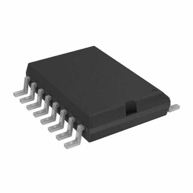
- Part No.:
- TC520ACOE
- Manufacturer:
- Microchip Technology
- Category:
- Specialized
- Package:
- 16-SOIC (0.295", 7.50mm Width)
- Datasheet:
-
 TC520ACOE.pdf
- Description:
- IC INTERFACE SPECIALIZED 16SOIC
- Quantity:
- Payment:

- Shipping:

Inventory:1,916
Please send an inquiry. Send us your inquiry, and we will respond immediately.
Product details
Overview
TC520ACOE from Microchip Technology is a serial interface adapter IC designed to manage phase control signals (A, B, CMPTR) for TC500/TC500A/TC510/TC514 dual-slope integrating A/D converters. It supports programmable conversion rate and resolution up to 17-bit accuracy plus polarity bit, operates from a single 5V supply, and delivers low power consumption (typically 0.8 mA). It enables polled or interrupt-mode host communication via a 3-wire serial port in portable data acquisition systems.
For engineers reviewing the TC520ACOE datasheet, TC520ACOE pinout, TC520ACOE application, or TC520ACOE equivalent, this device serves as a dedicated logic controller for precision dual-slope ADC interfacing-requiring attention to LOAD VALUE initialization, SYSCLK timing constraints (≤6 MHz external clock), DV interrupt synchronization, and CE-controlled conversion suspension.
Technical Context
The TC520ACOE integrates an 18-bit shift register, 16-bit counter, and state machine that sequences TC5XX A/D converter phases (Auto Zero, Integrate, De-integrate, Integrator Zero) using programmable LOAD VALUE. Its internal SYSCLK is derived by dividing OSCIN/OSCOUT input frequency by 4, supporting crystal (1–4 MHz) or external clock (up to 6 MHz).
Communication occurs over a 3-wire serial interface (DIN/DOUT/DCLK) with READ-activated data output and CE-gated conversion control. DV output signals data readiness at Auto Zero phase start, enabling either polling or IRQ-driven read cycles without requiring precise timing alignment to conversion completion.
Key Specifications
| Parameter | Value and Actual Design Meaning |
|---|---|
| Supply Voltage | 4.5 V to 5.5 V - ensures compatibility with standard 5V logic systems and stable operation across industrial temperature range. |
| Supply Current | 0.8 mA typical - enables battery-powered portable instrumentation without excessive power draw. |
| Crystal Frequency | 1.0–4.0 MHz - sets base timebase for integration timing; divided internally by 4 to generate SYSCLK. |
| External Clock Max | 6.0 MHz - allows higher-speed timing when using buffered pulse train instead of crystal. |
| Serial Clock Max | 3.0 MHz - defines maximum DCLK frequency for reliable DIN/DOUT bit transfer. |
| Resolution Support | Up to 17 bits (16 data + polarity + overrange) - provides high-precision digitization for low-noise analog measurement. |
| Operating Temp | 0°C to +70°C - validated for commercial-grade embedded data acquisition applications. |
Pinout & Package
TC520ACOE is housed in a 16-pin SOIC (Wide) package with 0.300-inch body width and standard 0.050-inch lead pitch. Pin 1 is marked by a notch or dot; pins are numbered counterclockwise from top-left corner.
| Pin/Terminal | Circuit Role | Design Meaning |
|---|---|---|
| VDD (Pin 1) | Power supply input | +5V ±10% digital supply referenced to DGND; powers all internal logic and I/O buffers. |
| DGND (Pin 2) | Digital ground reference | Return path for VDD and all digital signal currents; must be separated from analog ground in mixed-signal layouts. |
| CMPTR (Pin 3) | A/D comparator output interface | Accepts zero-crossing signal from TC5XX to terminate de-integrate phase; polarity depends on A/D input voltage sign. |
| B (Pin 4) | A/D phase control output | Drives TC5XX B input; combined with A, selects Auto Zero (01), Integrate (10), De-integrate (11), or Integrator Zero (00) mode. |
| A (Pin 5) | A/D phase control output | Drives TC5XX A input; binary combination with B determines converter operational phase sequence. |
| OSCOUT (Pin 6) | Crytal oscillator output | Connects to one side of AT-cut crystal (1–4 MHz); left floating when using external clock on OSCIN. |
| OSCIN (Pin 7) | Crytal oscillator input / external clock input | Connects to other side of crystal or accepts 30%–70% duty cycle pulse train up to 6 MHz for timebase generation. |
| N/C (Pin 8) | No connection | Not bonded internally; must remain unconnected on PCB. |
| N/C (Pin 9) | No connection | Not bonded internally; must remain unconnected on PCB. |
| READ (Pin 10) | Serial port enable input | Active-low level- and edge-triggered; loads 18-bit shift register and enables DOUT during low state. |
| DOUT (Pin 11) | Serial data output | Three-state output enabled only when READ is low; transmits OVR/POL/16-bit data MSB-first on DCLK falling edge. |
| DCLK (Pin 12) | Serial clock input | Positive- and negative-edge triggered; clocks data into DIN (rising edge) and out of DOUT (falling edge). |
| DIN (Pin 13) | Serial data input | Accepts LOAD VALUE byte (MSB first) to configure integration and auto-zero timing counters. |
| LOAD (Pin 14) | Timebase load strobe | Active-low level- and edge-triggered; transfers DIN value into internal 16-bit counter when released high. |
| DV (Pin 15) | Data valid indicator | Active-low open-drain output asserted at start of Auto Zero phase; used for polling or interrupt-driven data capture. |
| CE (Pin 16) | Conversion enable | Active-low level-triggered; halts conversion and forces Auto Zero when high; must be asserted only during DV = low. |
Key Features
| Feature | Design Value |
|---|---|
| Programmable LOAD VALUE | 8-bit upper byte configures 16-bit counter to set AZ/INT phase duration, directly trading resolution (up to 17-bit) against conversion speed. |
| 3-wire serial interface | Asynchronous DCLK-synchronized communication eliminates need for shared system clock and simplifies isolation in noisy environments. |
| DV output signaling | Hardware-generated active-low flag indicates start of new conversion cycle, enabling deterministic data read timing without polling status registers. |
| CE-controlled conversion suspension | Allows safe pause/resume of A/D conversion during multiplexer channel switching without integrator discharge errors. |
| Crystal or external clock support | Flexible timebase options (1–4 MHz crystal or ≤6 MHz external clock) accommodate layout constraints and EMI requirements. |
Applications
| Portable Data Loggers | Industrial Sensor Interfaces |
|---|---|
Use Scenario: Battery-powered handheld instruments measuring temperature, pressure, or humidity with microcontroller-based logging. IC Role / Device Role / Timing Role: Serial interface adapter managing TC514 dual-slope A/D converter timing and data serialization. Use Value: Enables 17-bit resolution measurements with <1.5 mA supply current, extending battery life while maintaining noise immunity through dual-slope integration. | Use Scenario: PLC analog input modules acquiring slow-varying process signals (e.g., 4–20 mA loop outputs) in factory automation. IC Role / Device Role / Timing Role: Dedicated phase sequencer and serial data formatter for TC500A A/D converter in isolated front-end circuitry. Use Value: Provides programmable integration time (via LOAD VALUE) to reject 50/60 Hz line noise and deliver stable readings under electrically noisy conditions. |
| Medical Instrumentation | Test & Measurement Equipment |
Use Scenario: Portable ECG or blood glucose meters requiring high-accuracy DC-coupled analog measurements. IC Role / Device Role / Timing Role: Logic controller coordinating TC510 A/D converter auto-zero and integrate phases to minimize offset drift. Use Value: Delivers consistent 16-bit+ linearity and <0.1% gain error by offloading timing-critical sequencing from host MCU. | Use Scenario: Benchtop multimeters or calibration sources needing stable, repeatable DC voltage digitization. IC Role / Device Role / Timing Role: Interface between microcontroller and TC500 dual-slope A/D core for precision DC measurement subsystem. Use Value: Supports user-selectable conversion rates (via LOAD VALUE) to balance measurement speed and resolution for different test modes. |
Equivalent & Alternatives
The following parts are listed as comparable options for similar serial A/D interface applications.
| Alternative Part | Technical Difference | Application Difference | Selection Advice |
|---|---|---|---|
| TC520ACPD | Same die, 14-pin PDIP package; lacks Pins 8 and 9 (N/C), shifts pin numbering for OSCOUT/OSCIN to Pins 6/7. | Used where through-hole assembly or prototyping on breadboard/perfboard is required. | Select TC520ACPD for legacy through-hole designs; verify PCB footprint and thermal dissipation limits differ from SOIC. |
| MAX132 | Complete 18-bit dual-slope A/D converter with integrated reference and serial interface; no external TC5XX required. | Replaces entire TC5XX + TC520A subsystem with single-chip solution; higher integration but less flexible timing control. | Choose MAX132 when minimizing component count is critical and fixed 18-bit resolution suffices; TC520ACOE retains configurability for custom integration times. |
Compared with TC520ACPD, TC520ACOE offers surface-mount reliability and smaller footprint; compared with MAX132, it preserves design flexibility for optimizing integration time and noise rejection in specialized sensor front-ends.
Availability
TC520ACOE is available at Aetrix Electronics and suitable for portable instruments, industrial sensor interfaces, and medical instrumentation requiring stable component supply and long-term obsolescence management.
Supply support for TC520ACOE includes scheduled delivery planning, volume procurement assistance, BOM continuity management, traceable sourcing, and lifecycle availability coordination for OEM customers, industrial embedded developers, connected-device designers, and electronics production programs.
Manufacturer
Microchip Technology Inc. is a U.S.-based semiconductor company specializing in microcontrollers, analog devices, and interface ICs for embedded control applications.
The TC520A product line was developed specifically to simplify integration of Microchip's TC500-family dual-slope A/D converters by handling timing-critical phase sequencing and serial data formatting in hardware.
FAQ
What is the primary function of the TC520ACOE in a data acquisition system?
The TC520ACOE acts as a dedicated serial interface adapter that manages phase control signals (A, B, CMPTR) for TC500/TC500A/TC510/TC514 dual-slope A/D converters. It relieves the host processor from real-time timing control, handles programmable integration time via LOAD VALUE, and formats conversion results into an 18-bit serial stream. This makes TC520ACOE essential for achieving high-precision, noise-immune DC measurements without burdening the main MCU.
How does the TC520ACOE achieve up to 17-bit resolution?
The TC520ACOE itself does not perform analog-to-digital conversion but enables up to 17-bit effective resolution (16 data bits + polarity + overrange) by precisely controlling the TC5XX A/D converter's integration and de-integration phases. Resolution is determined by the programmable LOAD VALUE, which sets the number of SYSCLK counts allocated to Auto Zero and Integrate phases-higher counts yield greater resolution at the cost of longer conversion time. The TC520ACOE shifts out the full 18-bit result (OVR/POL/data) serially upon READ activation.
Can the TC520ACOE operate without an external crystal?
Yes, the TC520ACOE can operate without an external crystal by using an external clock source applied to the OSCIN pin (with OSCOUT left floating). The device accepts a pulse train up to 6 MHz with ≥30% duty cycle, ≤15 ns rise/fall times, and 0–VIH amplitude. This option provides layout flexibility and avoids crystal-related EMI or startup delay issues, though crystal operation (1–4 MHz) offers better frequency stability for precision metrology applications.
What is the role of the DV pin on the TC520ACOE?
The DV (Data Valid) pin on the TC520ACOE is an active-low output that goes low at the start of each Auto Zero phase-indicating that the previous conversion's 18-bit result is fully loaded into the internal shift register and ready for serial readout. It serves as a hardware handshake signal, enabling either polling (checking DV before READ) or interrupt-driven operation (connecting DV to MCU IRQ). This eliminates guesswork about conversion completion timing and ensures deterministic data capture.
How is the LOAD VALUE initialized and updated on the TC520ACOE?
The LOAD VALUE is an 8-bit configuration byte that sets the upper byte of the TC520ACOE's 16-bit timebase counter, determining integration and auto-zero durations. It is initialized at power-up by shifting the byte MSB-first into DIN while LOAD is held low, then releasing LOAD high to latch it. The value can be reloaded dynamically during operation-e.g., during DV = low-to adapt integration time for different input ranges or noise environments. TC520ACOE does not retain LOAD VALUE across power cycles; reinitialization is mandatory after reset.
TC520ACOE Specifications
- Product attributes
- Attribute value
- Manufacturer:
- Microchip Technology
- Series:
- -
- Package/Case:
- 16-SOIC (0.295", 7.50mm Width)
- Packaging:
- Tube
- Product Status:
- Active
- Applications:
- Computer Peripheral Interface, Data Acquisition System Interface, Portable Instruments
- Interface:
- Serial
- Voltage - Supply:
- 4.5V ~ 5.5V
- Supplier Device Package:
- 16-SOIC
- Grade:
- -
- Qualification:
- -
- Mounting Type:
- Surface Mount
TC520ACOE FAQ
1.How can I place an order for TC520ACOE through Aetrix?
Please submit a Request for Quotation (RFQ) for TC520ACOE on Aetrix. Our sales agent will provide a competitive quotation and guide you through the order confirmation once you accept the terms.
2.Are the price and stock information for TC520ACOE reliable?
The price and inventory of TC520ACOE are updated periodically and may fluctuate due to market conditions. Stock and pricing data are typically refreshed every 24 hours. Quotation validity for TC520ACOE is usually 5 days.
3.What payment methods are accepted for TC520ACOE?
We accept Wire Transfer, PayPal, Credit Card, Western Union, MoneyGram, and Escrow for TC520ACOE transactions.
Note: Certain payment methods may incur a processing fee.
4.How is shipping managed for TC520ACOE?
TC520ACOE orders can be shipped via leading logistics carriers, including DHL, UPS, FedEx, TNT, or Registered Mail.
Once your TC520ACOE order is processed, you will receive an email with the shipment details and tracking number.
Note: Tracking information may take up to 24 hours to appear. Express delivery typically takes 3–5 business days.
5.How can I obtain technical support or documentation for TC520ACOE?
For technical support, including TC520ACOE datasheets, pinout diagrams, or application guidance, please contact our engineering support team. They can provide detailed documentation and assistance for your TC520ACOE requirements.
6.How does Aetrix verify that TC520ACOE is sourced from the original manufacturer or authorized distributors?
All TC520ACOE products on Aetrix are procured from qualified distributors and authorized channels. Our dedicated quality assurance team conducts strict verification, including traceability checks and, if necessary, third-party testing. This ensures that TC520ACOE meets industry standards.
7.What is the process for return or replacement of TC520ACOE?
All TC520ACOE units undergo pre-shipment inspection (PSI). If there is an issue with TC520ACOE, returns or replacements are accepted under the following conditions:
1.Quantity discrepancies, incorrect items, or visible external defects (such as breakage or corrosion), acknowledged by Aetrix.
2.The issue is reported within 90 days of delivery.
3.The TC520ACOE part is unused and in its original packaging.
Return procedure for TC520ACOE:
1.Submit a request within 90 days.
2.Obtain a Return Material Authorization (RMA) from Aetrix.
TC520ACOE Tags

-
NVT4857UKAZ
NXP Semiconductors

-
TCA8418RTWR
Texas Instruments

-
PCA9546APWR
Texas Instruments

-
MD0100N8-G
Microchip Technology

-
PCA9548APW,118
NXP Semiconductors

-
PCA9540BDP,118
NXP Semiconductors

-
PCA9548APWR
Texas Instruments

-
PCA9546APW,118
NXP Semiconductors

-
PTN3360DBS,518
NXP Semiconductors

-
PCA9546ABS,118
NXP Semiconductors

-
PCA9518PWR
Texas Instruments

-
PCA9545APW,118
NXP Semiconductors
Tech Hub

TTL and CMOS logic families differ in thresholds, loading, output drive, power and timing. This engineering guide compares 74HC and 74HCT, calculates noise margins and checks 3.3 V/5 V compatibility.

A practical engineering guide to 3.3V and 5V logic compatibility, input thresholds, resistor dividers, translator ICs, MOSFET level shifting, I2C pull-ups, timing limits and power-sequencing risks.

The 74HC595 uses push-pull logic outputs, while the TPIC6B595 uses 50 V open-drain DMOS sinks for higher-power loads. This guide compares timing, current limits, 3.3 V interfacing, load wiring, thermal…

The 74HC595 converts serial data into eight stable parallel outputs. This guide covers pin functions, shift and storage timing, OE and MR behavior, drive-current limits, cascading, voltage compatibilit…

A technical comparison of level-sensitive latches and edge-triggered flip-flops, covering timing windows, setup and hold limits, master–slave operation, time borrowing, race-through, HDL inference and…

A D latch stores one bit while Enable controls when data can pass. This reference covers gate-level operation, truth tables, transparency, setup and hold timing, LE versus OE, common ICs and practical …

An SR latch stores one bit through cross-coupled feedback. This engineering reference covers NOR and NAND implementations, truth tables, forbidden-state recovery, gated operation, switch debouncing, fa…

Latch circuits retain one bit through feedback. This technical reference covers SR and D latches, truth tables, transparency, timing limits, latch-versus-flip-flop behavior, applications and common log…

An engineering guide to LED driver operation, constant-current and constant-voltage outputs, linear and switching topologies, dimming, IC selection, calculations, replacement compatibility, and fault c…

Operational amplifier guide covering op amp basics, feedback, ideal vs real op amps, common configurations, buffer circuits, offset, bias current, gain-bandwidth, slew rate, rail-to-rail limits and sel…


