
 My Inquiry
 My Account


Microchip Technology TC520ACOE713
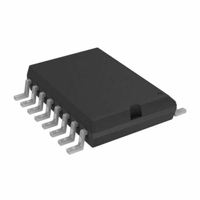
- Part No.:
- TC520ACOE713
- Manufacturer:
- Microchip Technology
- Category:
- Specialized
- Package:
- 16-SOIC (0.295", 7.50mm Width)
- Datasheet:
-
 TC520ACOE713.pdf
- Description:
- IC INTERFACE SPECIALIZED 16SOIC
- Quantity:
- Payment:

- Shipping:

Inventory:1,471
Please send an inquiry. Send us your inquiry, and we will respond immediately.
Product details
Overview
TC520ACOE713 from Microchip Technology is a serial interface adapter IC designed to manage phase control signals (A, B, CMPTR) for TC500/TC500A/TC510/TC514 dual-slope integrating A/D converters. It provides 18-bit serial data output (16-bit conversion + polarity + overrange), supports programmable integration/auto-zero timing via LOAD VALUE byte, and operates with 5V supply at ≤0.8mA typical current draw. Used in portable instruments and computer peripheral interfaces requiring high-accuracy analog-to-digital conversion.
For engineers reviewing the TC520ACOE713 datasheet, TC520ACOE713 pinout, TC520ACOE713 application, or TC520ACOE713 equivalent, this device serves as a dedicated logic controller for dual-slope ADC families - enabling polled or interrupt-driven serial readout, external crystal or 6MHz clock input, and flexible resolution/speed trade-off through 8-bit LOAD VALUE programming.
Technical Context
The TC520ACOE713 implements an internal 16-bit counter with fixed LSB (0xFF) and programmable MSB (LOAD VALUE), generating SYSCLK-derived timing for Auto Zero (AZ) and Integrate (INT) phases of connected TC5xx converters. Its state machine sequences A/B outputs to drive TC5xx phase transitions (AZ/INT/DINT/IZ) and monitors CMPTR to terminate de-integration.
Communication occurs over a 3-wire serial port (DIN/DOUT/DCLK) with READ-controlled shift register access and DV-driven interrupt signaling. The device accepts external clock up to 6MHz or 1–4MHz crystal between OSCIN/OSCOUT, dividing by 4 to produce SYSCLK; all internal timing-including TAZI (100ms power-up auto-zero), TRD (250ns READ delay), and TPWL/TPWH (150ns DCLK pulse widths)-is derived from this source.
Key Specifications
| Parameter | Value and Actual Design Meaning |
|---|---|
| Supply Voltage | 4.5V to 5.5V - compatible with standard 5V logic systems; no level-shifting required |
| Supply Current | 0.8mA typical - enables low-power portable instrumentation designs |
| Serial Clock Max | 3MHz DCLK - supports fast host processor readout without timing margin violation |
| Crystal Frequency | 1.0–4.0MHz - sets base timing resolution for AZ/INT phase duration control |
| Data Output Format | OVR + POL + 16-bit MSB-first - delivers signed 17-bit result with overrange flag for error detection |
| Conversion Trigger | CE active-low level - halts conversion and forces AZ mode when high; requires synchronization with DV low |
| Input Logic Levels | VIL ≤0.8V, VIH ≥2.0V - ensures robust noise immunity in mixed-signal industrial environments |
Pinout & Package
TC520ACOE713 is housed in a 16-pin SOIC (Wide) package with 0.300-inch body width and 1.27mm pitch. Pin 1 is marked by a beveled corner; pins 8 and 9 are no-connect (N/C). All I/Os are 5V-tolerant with CMOS-compatible thresholds.
| Pin/Terminal | Circuit Role | Design Meaning |
|---|---|---|
| VDD (Pin 1) | Power supply input | +5V ±10% digital supply; decoupling capacitor required near pin |
| DGND (Pin 2) | Digital ground reference | Return path for all digital I/O; must be separated from analog ground in mixed-signal layouts |
| CMPTR (Pin 3) | Zero-crossing comparator input | Signals integrator output crossing zero; high-to-low transition ends de-integrate phase |
| B (Pin 4) | TC5xx phase control output | Drives TC5xx B input; combined with A defines AZ/INT/DINT/IZ converter state |
| A (Pin 5) | TC5xx phase control output | Drives TC5xx A input; binary pair (A,B) selects conversion phase per TC5xx datasheet |
| OSCOUT (Pin 6) | Clock source connection | Connects to one side of AT-cut crystal (1–4MHz); float if using external clock on OSCIN |
| OSCIN (Pin 7) | Clock source connection | Connects to other crystal terminal or external 6MHz max pulse train; duty cycle ≥30% |
| READ (Pin 10) | Serial read strobe | Active-low; loads 18-bit shift register and enables DOUT; high-impedance when high |
| DOUT (Pin 11) | Serial data output | Outputs OVR/POL/MSB…LSB on falling DCLK edges; only active during READ low |
| DCLK (Pin 12) | Serial clock input | Positive/negative edge-triggered; clocks data into DIN (rising) and out of DOUT (falling) |
| DIN (Pin 13) | Serial data input | Accepts LOAD VALUE byte (MSB first) to configure AZ/INT timing counter MSB |
| LOAD (Pin 14) | LOAD VALUE latch control | Active-low; transfers DIN value into internal timebase counter when released high |
| DV (Pin 15) | Data valid indicator | Active-low open-drain output; asserts at start of AZ phase, usable as IRQ signal |
| CE (Pin 16) | Conversion enable | Active-low level-triggered; continuous conversion while low; forces AZ when high |
Key Features
| Feature | Design Value |
|---|---|
| Programmable AZ/INT timing | 8-bit LOAD VALUE sets counter MSB (0x00–0xFF), enabling resolution/speed tuning from 256 to 65536 SYSCLK counts per phase |
| 18-bit serial data format | OVR + POL + 16-bit conversion word delivered MSB-first - supports signed magnitude interpretation and overrange detection |
| Dual clock source support | Accepts either 1–4MHz crystal (OSCIN/OSCOUT) or up to 6MHz external clock (OSCIN only) - simplifies system clock architecture |
| Interrupt-capable DV output | Active-low signal synchronized to AZ phase start - directly connects to MCU IRQ line for zero-latency data ready notification |
| Polled or interrupt operation | No hardware dependency on interrupt controller; DV optional - ideal for resource-constrained microcontrollers or FPGA-based systems |
| Opto-isolation ready | 3-wire serial interface (DIN/DOUT/DCLK) and level-triggered CE/READ allow clean isolation barrier implementation with minimal extra components |
Applications
| Computer Peripheral Interface | Portable Instruments |
|---|---|
Use Scenario: Integrating analog sensor data (e.g., temperature, pressure) into legacy ISA/PCI bus peripherals with limited GPIO resources. IC Role / Device Role / Timing Role: Serial interface adapter managing TC514 phase sequencing and delivering digitized results over minimal 3-wire bus. Use Value: Reduces host CPU overhead by offloading TC514 timing control and eliminating software-based phase management loops. |
Use Scenario: Battery-powered handheld multimeter requiring high-precision DC voltage measurement with >16-bit effective resolution. IC Role / Device Role / Timing Role: Timing controller and serial data formatter for TC500A dual-slope converter, enabling low-noise integration with user-selectable speed/resolution. Use Value: Achieves 17-bit signed output with built-in polarity and overrange flags - eliminates need for external sign extension or fault monitoring logic. |
| Data Acquisition System Interface | Industrial Process Monitoring |
Use Scenario: Modular DAQ module acquiring multiple analog channels via multiplexer, requiring precise timing coordination and low EMI susceptibility. IC Role / Device Role / Timing Role: Centralized TC5xx sequencer with CE-gated conversion suspension during channel switching and DV-synchronized data capture. Use Value: Enables glitch-free channel scanning by halting conversion mid-cycle (via CE high during DV low) without integrator discharge errors. |
Use Scenario: Factory-floor PLC analog input card measuring 4–20mA loop signals with high common-mode rejection and long-term stability. IC Role / Device Role / Timing Role: Dual-slope ADC controller providing inherent 50/60Hz noise rejection via programmable integration time aligned to AC line cycles. Use Value: Supports LOAD VALUE configuration for exact 100ms or 83.3ms integration periods - achieving optimal power-line interference cancellation. |
Equivalent & Alternatives
The following parts are listed as comparable options for similar serial interface adapter applications.
| Alternative Part | Technical Difference | Application Difference | Selection Advice |
|---|---|---|---|
| TC520ACPD | 14-pin PDIP package; identical electrical specs and pin functions except missing N/C pins 8 and 9; same 0°C to +70°C temp range | Preferred for through-hole prototyping or legacy PCBs with PDIP footprints; lacks SOIC thermal performance and density | Select TC520ACPD only when board layout or assembly process mandates DIP packaging - no functional difference in operation or timing. |
| MAX1241ACPP+ | 12-bit serial ADC with integrated reference; SPI interface; no external TC5xx dependency; 2.7–5.25V supply; 75μA quiescent current | Suitable for lower-resolution, self-contained measurements where dual-slope architecture and ultra-high linearity are not required | Choose MAX1241ACPP+ for compact, low-power single-chip solutions - but not as a drop-in replacement for TC520ACOE713's TC5xx control functionality. |
Compared with TC520ACOE713, TC520ACPD offers identical functionality in a through-hole package but sacrifices board space efficiency, while MAX1241ACPP+ provides integrated conversion at lower resolution and eliminates the need for external dual-slope converters - making it suitable only for applications abandoning TC5xx-based high-accuracy architectures.
Availability
TC520ACOE713 is available at Aetrix Electronics and suitable for computer peripheral interface, portable instrumentation, and industrial data acquisition systems requiring stable component supply across extended production lifecycles.
Supply support for TC520ACOE713 includes scheduled delivery planning, volume procurement assistance, BOM continuity management, traceable sourcing, and lifecycle availability coordination for OEM customers, industrial embedded developers, connected-device designers, and electronics production programs.
Manufacturer
Microchip Technology is a U.S.-based semiconductor company specializing in microcontrollers, analog devices, and interface ICs, with ISO/TS-16949 certified manufacturing facilities.
The TC520A product line was engineered specifically to simplify system integration of Microchip's TC500-family dual-slope A/D converters - reducing firmware complexity and improving measurement repeatability in precision analog applications.
FAQ
What is the primary function of the TC520ACOE713 in a data acquisition system?
The TC520ACOE713 acts as a dedicated serial interface adapter that manages phase control signals (A, B, CMPTR) for TC500/TC500A/TC510/TC514 dual-slope A/D converters. It handles timing, initiates conversions via CE, formats 18-bit serial output (OVR/POL/data), and supports both polled and interrupt-driven host communication - significantly reducing software overhead in precision DAQ systems using TC5xx converters.
Can the TC520ACOE713 operate without an external crystal?
Yes, the TC520ACOE713 can operate without an external crystal by using an external clock signal up to 6MHz applied to the OSCIN pin, with OSCOUT left floating. The internal divider-by-4 generates SYSCLK for all timing functions. Crystal operation (1–4MHz between OSCIN/OSCOUT) is optional and used when higher frequency stability or lower jitter is required for critical integration timing.
How does the LOAD VALUE byte affect conversion performance in the TC520ACOE713?
The LOAD VALUE byte (loaded via DIN/LOAD) sets the most significant byte of the TC520ACOE713's 16-bit timebase counter, directly determining the number of SYSCLK cycles allocated to Auto Zero and Integrate phases. Higher values increase resolution (up to 17 bits) but slow conversion speed; lower values improve throughput at reduced accuracy - enabling precise trade-off tuning for each application's noise and speed requirements.
Is the TC520ACOE713 pin-compatible with other variants in the TC520A family?
The TC520ACOE713 (16-pin SOIC) shares identical signal mapping and electrical behavior with TC520ACPD (14-pin PDIP), except pins 8 and 9 are N/C in the SOIC version and absent in PDIP. Both use the same VDD/DGND/CMPTR/A/B/OSCIN/OSCOUT/READ/DOUT/DCLK/DIN/LOAD/DV/CE pin functions - making them functionally interchangeable with minor PCB layout adaptation for package type.
What happens to the TC520ACOE713 when the CE pin is pulled high during conversion?
When CE is pulled high, the TC520ACOE713 immediately halts the current conversion cycle and forces the connected TC5xx A/D converter into Auto Zero (AZ) mode. The DV output goes low to indicate AZ entry, and the device remains in AZ until CE is returned low. This feature allows safe multiplexer channel switching without integrator discharge errors - but CE must only be asserted when DV is low to prevent measurement corruption.
TC520ACOE713 Specifications
- Product attributes
- Attribute value
- Manufacturer:
- Microchip Technology
- Series:
- -
- Package/Case:
- 16-SOIC (0.295", 7.50mm Width)
- Packaging:
- Tape & Reel (TR)
- Product Status:
- Obsolete
- Applications:
- Computer Peripheral Interface, Data Acquisition System Interface, Portable Instruments
- Interface:
- Serial
- Voltage - Supply:
- 4.5V ~ 5.5V
- Supplier Device Package:
- 16-SOIC
- Grade:
- -
- Qualification:
- -
- Mounting Type:
- Surface Mount
TC520ACOE713 FAQ
1.How can I place an order for TC520ACOE713 through Aetrix?
Please submit a Request for Quotation (RFQ) for TC520ACOE713 on Aetrix. Our sales agent will provide a competitive quotation and guide you through the order confirmation once you accept the terms.
2.Are the price and stock information for TC520ACOE713 reliable?
The price and inventory of TC520ACOE713 are updated periodically and may fluctuate due to market conditions. Stock and pricing data are typically refreshed every 24 hours. Quotation validity for TC520ACOE713 is usually 5 days.
3.What payment methods are accepted for TC520ACOE713?
We accept Wire Transfer, PayPal, Credit Card, Western Union, MoneyGram, and Escrow for TC520ACOE713 transactions.
Note: Certain payment methods may incur a processing fee.
4.How is shipping managed for TC520ACOE713?
TC520ACOE713 orders can be shipped via leading logistics carriers, including DHL, UPS, FedEx, TNT, or Registered Mail.
Once your TC520ACOE713 order is processed, you will receive an email with the shipment details and tracking number.
Note: Tracking information may take up to 24 hours to appear. Express delivery typically takes 3–5 business days.
5.How can I obtain technical support or documentation for TC520ACOE713?
For technical support, including TC520ACOE713 datasheets, pinout diagrams, or application guidance, please contact our engineering support team. They can provide detailed documentation and assistance for your TC520ACOE713 requirements.
6.How does Aetrix verify that TC520ACOE713 is sourced from the original manufacturer or authorized distributors?
All TC520ACOE713 products on Aetrix are procured from qualified distributors and authorized channels. Our dedicated quality assurance team conducts strict verification, including traceability checks and, if necessary, third-party testing. This ensures that TC520ACOE713 meets industry standards.
7.What is the process for return or replacement of TC520ACOE713?
All TC520ACOE713 units undergo pre-shipment inspection (PSI). If there is an issue with TC520ACOE713, returns or replacements are accepted under the following conditions:
1.Quantity discrepancies, incorrect items, or visible external defects (such as breakage or corrosion), acknowledged by Aetrix.
2.The issue is reported within 90 days of delivery.
3.The TC520ACOE713 part is unused and in its original packaging.
Return procedure for TC520ACOE713:
1.Submit a request within 90 days.
2.Obtain a Return Material Authorization (RMA) from Aetrix.
TC520ACOE713 Tags

-
NVT4857UKAZ
NXP Semiconductors

-
TCA8418RTWR
Texas Instruments

-
PCA9546APWR
Texas Instruments

-
MD0100N8-G
Microchip Technology

-
PCA9548APW,118
NXP Semiconductors

-
PCA9540BDP,118
NXP Semiconductors

-
PCA9548APWR
Texas Instruments

-
PCA9546APW,118
NXP Semiconductors

-
PTN3360DBS,518
NXP Semiconductors

-
PCA9546ABS,118
NXP Semiconductors

-
PCA9518PWR
Texas Instruments

-
PCA9545APW,118
NXP Semiconductors
Tech Hub

TTL and CMOS logic families differ in thresholds, loading, output drive, power and timing. This engineering guide compares 74HC and 74HCT, calculates noise margins and checks 3.3 V/5 V compatibility.

A practical engineering guide to 3.3V and 5V logic compatibility, input thresholds, resistor dividers, translator ICs, MOSFET level shifting, I2C pull-ups, timing limits and power-sequencing risks.

The 74HC595 uses push-pull logic outputs, while the TPIC6B595 uses 50 V open-drain DMOS sinks for higher-power loads. This guide compares timing, current limits, 3.3 V interfacing, load wiring, thermal…

The 74HC595 converts serial data into eight stable parallel outputs. This guide covers pin functions, shift and storage timing, OE and MR behavior, drive-current limits, cascading, voltage compatibilit…

A technical comparison of level-sensitive latches and edge-triggered flip-flops, covering timing windows, setup and hold limits, master–slave operation, time borrowing, race-through, HDL inference and…

A D latch stores one bit while Enable controls when data can pass. This reference covers gate-level operation, truth tables, transparency, setup and hold timing, LE versus OE, common ICs and practical …

An SR latch stores one bit through cross-coupled feedback. This engineering reference covers NOR and NAND implementations, truth tables, forbidden-state recovery, gated operation, switch debouncing, fa…

Latch circuits retain one bit through feedback. This technical reference covers SR and D latches, truth tables, transparency, timing limits, latch-versus-flip-flop behavior, applications and common log…

An engineering guide to LED driver operation, constant-current and constant-voltage outputs, linear and switching topologies, dimming, IC selection, calculations, replacement compatibility, and fault c…

Operational amplifier guide covering op amp basics, feedback, ideal vs real op amps, common configurations, buffer circuits, offset, bias current, gain-bandwidth, slew rate, rail-to-rail limits and sel…


